Semiconductor device having metal foil integral with sealing resin

Inactive Publication Date: 2000-02-08
NITTO DENKO CORP
View PDF5 Cites 25 Cited by
  • Summary
  • Abstract
  • Description
  • Claims
  • Application Information

AI Technical Summary

Problems solved by technology

As known, to solder a semiconductor device sealed with a resin, it is feared that the moisture content absorbed to a sealing resin layer during the storage of the semiconductor device may be evaporated by heating at the soldering time and that cracks may occur in the sealing resin layer due to the vapor pressure.
This phenomenon occurs because the strength of the sealing resin material heated to the soldering temperature (high-temperature strength) cannot endure the vapor pressure.
However, if the high-temperature strength of the sealing resin material is enhanced to prevent cracks from occurring in the sealing resin layer, the glass transition temperature of the sealing resin material rises accordingly and the moisture absorption percentage rises, leading to an unavoidable rise in the vapor pressure.
On the other hand, if the moisture absorption percentage of the sealing resin material is lowered, the glass transition temperature lowers accordingly, resulting in unavoidable degradation of the high-temperature strength of the sealing resin material.
Therefore, there is a limit to selection of the sealing resin material itself to prevent crack occurrence in the sealing resin layer caused by heating at the soldering time.
However, to use metal foil as a water blocking layer of the sealing resin layer of the semiconductor device

Method used


Image

  • Semiconductor device having metal foil integral with sealing resin
  • Semiconductor device having metal foil integral with sealing resin
  • Semiconductor device having metal foil integral with sealing resin

Examples


Example

First Comparative Example

A first comparative example was the same as the first example except that copper foil was not used.

Example

Second Comparative Example

A manufactured semiconductor device from the first comparative example was covered with copper foil by epoxy bonding example.

To evaluate crack resistance of the sealing resin layer at the soldering time for the example and comparative example articles (the number of specimens is each 10), the specimens were left alone for 480 hours at a temperature of 85.degree. C. and a humidity of 85%, then were heated with vapor at 215.degree. C. and whether or not cracks occurred was checked. No cracks were observed on the example articles. In contrast, cracks were recognized on five of the ten articles in the first comprative example and two of the ten articles in the second comparative example.

From the test results, particularly from the comparison between the test results of the first example and the second comprative example, it can be estimated that the semiconductor device according to the invention can well exclude occurrence of a thermal stress in the sealing re...

Example

Second Example

A polycarbodiimide composition was used as a sealing resin material and to compound the polycarbodiimide composition, 2, 2-bis [4-(4-isocyanate phenoxy) phenyl] hexafluoropropane 500 g, tetrahydrofuran 2500 milliliters, and a carbodiimide catalyst 1.35 g were poured into a 5000-milliliter four-necked flask comprising a thermometer, an agitator, and a calcium chloride tube and were agitated at 60.degree. C. for 6.5 hours to produce a polycarboimide solution having molecular weight of about 8,300. This reaction liquid was poured into isopropyl alcohol and a precipitated polymer was isolated by filtering and was dried, thereby producing a polycarbodiimide composition.

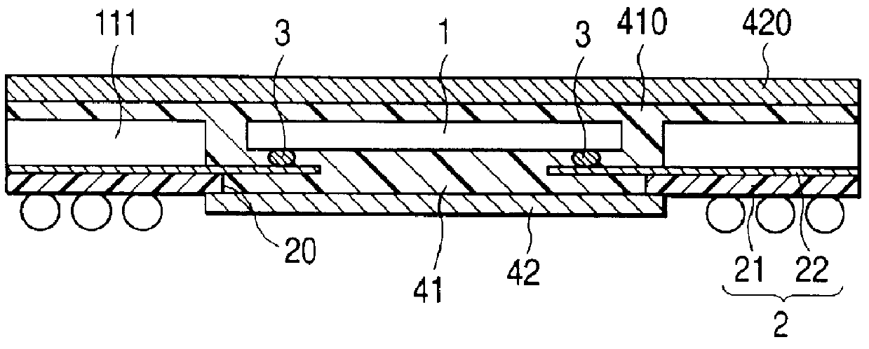
A manufactured semiconductor device has the configuration shown in FIG. 1. A semiconductor element about 6 mm.times.6 mm was mounted by bump junction on conductor wiring of carrier tape before a wiring base material is punched. A polycarbodiimide sealing resin and copper foil laminate with plane dimensions 7 ...


PUM


Abstract

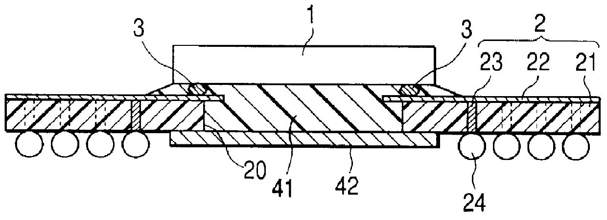
A semiconductor device with a metal foil and a sealing resin material. Metal foil is formed integrally with the sealing resin layer.

Description

1. Field of the InventionThis invention relates to a manufacturing method of a semiconductor device using a wiring base material having conductor wiring on an insulating film as an electric path from a semiconductor element to the outside and the semiconductor device provided by sealing with a resin shows excellent resistance to cracks of soldering on the printed circuit board.2. Description of the Related ArtA tape carrier type semiconductor device or a tape ball grid array type semiconductor device is known as a semiconductor device using a wiring base material having conductor wiring on an insulating film as an electric path from a semiconductor element to the outside. Further, a semiconductor device comprising a metal radiator plate brought into contact with a semiconductor element of a tape carrier type semiconductor device is also known.FIG. 4 shows an example of the tape carrier type semiconductor device. An electrode of a semiconductor element 1' is connected with a wiring c...

Claims


Application Information

Patent Timeline
IPC IPC(8): H01L23/48H01L23/31H01L23/58H01L23/28H01L23/498H01L21/60H01L23/12H01L23/29
CPCH01L23/3107H01L23/49816H01L23/585H01L2224/16H01L2924/0102H01L2924/01078H01L2924/01079H01L2924/15311
Inventor HOTTA, YUJIMOCHIZUKI, AMANESAKAMOTO, MICHIEYOSHIOKA, MASAHIRO
Owner NITTO DENKO CORP
Why Eureka
Try Eureka