Natural-superlattice homologous single crystal thin film, method for preparation thereof, and device using said single crystal thin film

a single crystal, natural superlattice technology, applied in the direction of crystal growth process, polycrystalline material growth, chemistry apparatus and processes, etc., can solve the problems of irregularity having considerable adverse effects, and achieve excellent insulation performance, excellent switching characteristic, and small deviation

Inactive Publication Date: 2006-06-13
HOYA CORP +1
View PDF11 Cites 4242 Cited by
  • Summary
  • Abstract
  • Description
  • Claims
  • Application Information

AI Technical Summary

Benefits of technology

[0020]Each of the layers in a superlattice structure has an extremely thin thickness of 1 to 100 atomic layers. Thus, if one of the layers locally has irregularity in thickness even at the atomic-layer level, such irregularity will have considerable adverse affects. Thus, in the production of such a superlattice structure, it is essential to control superlattice growth in the atomic-layer level through a sophisticated film-deposition technology, such as more advanced MBE process or CVD process. From this point of view, it is expected that if a superlattice existing in the natural is positively used instead of the aforementioned artificially prepared superlattice, a superlattice structure having an accurately controlled layer thickness can be prepared while simplifying the film-deposition process.
[0021]It is also expected that a natural superlattice structure has a potential for allowing one-dimensional superlattice structure (quantum wire structure) to be formed as well as two-dimensional superlattice structure (quantum well structure), and for allowing the range of applicable chemical compositions to be extended to oxides and others.
[0043]In the method set forth in the fourth aspect of the present invention, the thermal anneal treatment may be performed while covering the deposited film with a high-melting-point compound to prevent the vaporization of ZnO component from the deposited film.
[0044]The thermal anneal treatment may also be performed under the presence of ZnO vapor to prevent the vaporization of ZnO component from the deposited film.
[0051]The single crystal thin film of homologous compound containing ZnO as a primary component is transparent to visible light, and usable as a device constituting a transparent electronic circuit. The thin-film field-effect transistor of the present invention uses this single crystal thin film as an active layer. The homologous compound single crystal thin film can provide a new field-effect transistor having the following characteristics (1) to (3) superior to the conventional field-effect transistor using silicon.
[0054](3) A homologous compound InMO3 (ZnO)m (M=In, Fe, Ga or Al, and m=an integer in the range of 1 to less than 50) single-crystal thin film prepared through a reactive solid-phase epitaxy process has an extremely small deviation from the stoichiometric composition, and exhibits an excellent insulation performance around room temperature. Thus, the homologous compound InMO3 (ZnO)m (M=In, Fe, Ga or Al, and m=an integer in the range of 1 to less than 50) thin film can be used to produce a transparent thin-film field-effect transistor excellent in switching characteristic in a normally-off operation.

Problems solved by technology

Thus, if one of the layers locally has irregularity in thickness even at the atomic-layer level, such irregularity will have considerable adverse affects.

Method used


Image

  • Natural-superlattice homologous single crystal thin film, method for preparation thereof, and device using said single crystal thin film
  • Natural-superlattice homologous single crystal thin film, method for preparation thereof, and device using said single crystal thin film
  • Natural-superlattice homologous single crystal thin film, method for preparation thereof, and device using said single crystal thin film

Examples


example 1

[0085]The present invention will be described in more detail in connection with the following Examples.

[0086]1. Formation of ZnO Thin Film

[0087]A ZnO thin film was grown on a YAS (111) single-crystal substrate (10 square mm×0.5 mm t) at a substrate temperature of 800° C. Through a PLD process, a KrF (248 nm) excimer laser was irradiated to a target of ZnO sintered body in a vacuum chamber set at an oxygen pressure of 3×10⁻³ Pa to vaporize ZnO, and the ZnO was deposited on the YAS (111) single-crystal substrate heated at 800° C., at a deposition speed of 2 nm / min for 1 hour to form the ZnO thin film. According to the analysis of the prepared ZnO thin film by means of a high-resolution X-ray diffraction (HRXRD) technique, ZnO was deposited on the YSZ (111) substrate in (0001) orientation at a tilt angle of 0.02 to 0.1 degrees. Further, through an In-plain measurement, it was verified that the ZnO was epitaxially grown adequately. The epitaxial relationship between the ZnO and the subs...

example 2

[0099]In was selected as M1M2, and grown on the ZnO epitaxial thin film formed in the manner described in Example 1 to form an In2O3 thin film. Then, through a PLD process, a KrF (248 nm) excimer laser was irradiated to a target of In2O3 sintered body in a vacuum chamber set at an oxygen pressure of 3 ×10⁻³ Pa to vaporize In2O3, and the In2O3 was deposited on the YSZ (111) single-crystal substrate heated at 600° C., at a deposition speed of 2 nm / mm for 30 minutes to form the In2O3 thin film. The In2O3 was heteroepitaxially grown on the ZnO thin film, and the epitaxial relationship therebetween was as follows:

In2O3 (111) / / ZnO (0001) / / YSZ(111)

In2O3 (110) / / ZnO (11–20) / / YSZ(1–10).

[0100]The formed bilayer thin film was subjected to a thermal anneal treatment at 1300° C. in the atmosphere for 20 minutes, in the manner as described in Example 1. As a result, the formation of an epitaxial thin film of In2O3 (ZnO3)4, In2O3 (ZnO3)5 and In2O3 (ZnO3)6 which were mixed up was confirmed through a...

example 3

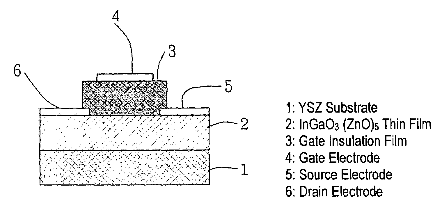
1. Formation of Single Crystal InGaO3 (ZnO)5 Thin Crystal

[0105]A ZnO thin film having a thickness of 2 mm was epitaxially grown on a YSZ (111) single-crystal substrate through a PLD process at a substrate temperature of 700° C. Then, after the substrate temperature was reduced to room temperature, a polycrystal InGaO3 (ZnO)5 thin film having a thickness of 150 nm was deposited on the ZnO epitaxial thin film through a PLD process. The formed bilayer thin film was taken out to the atmosphere, and subjected to a thermal anneal treatment using an electric furnace at 1400° C. in the atmosphere for 30 minutes. After the completion of the treatment, the treated film was cooled to room temperature.

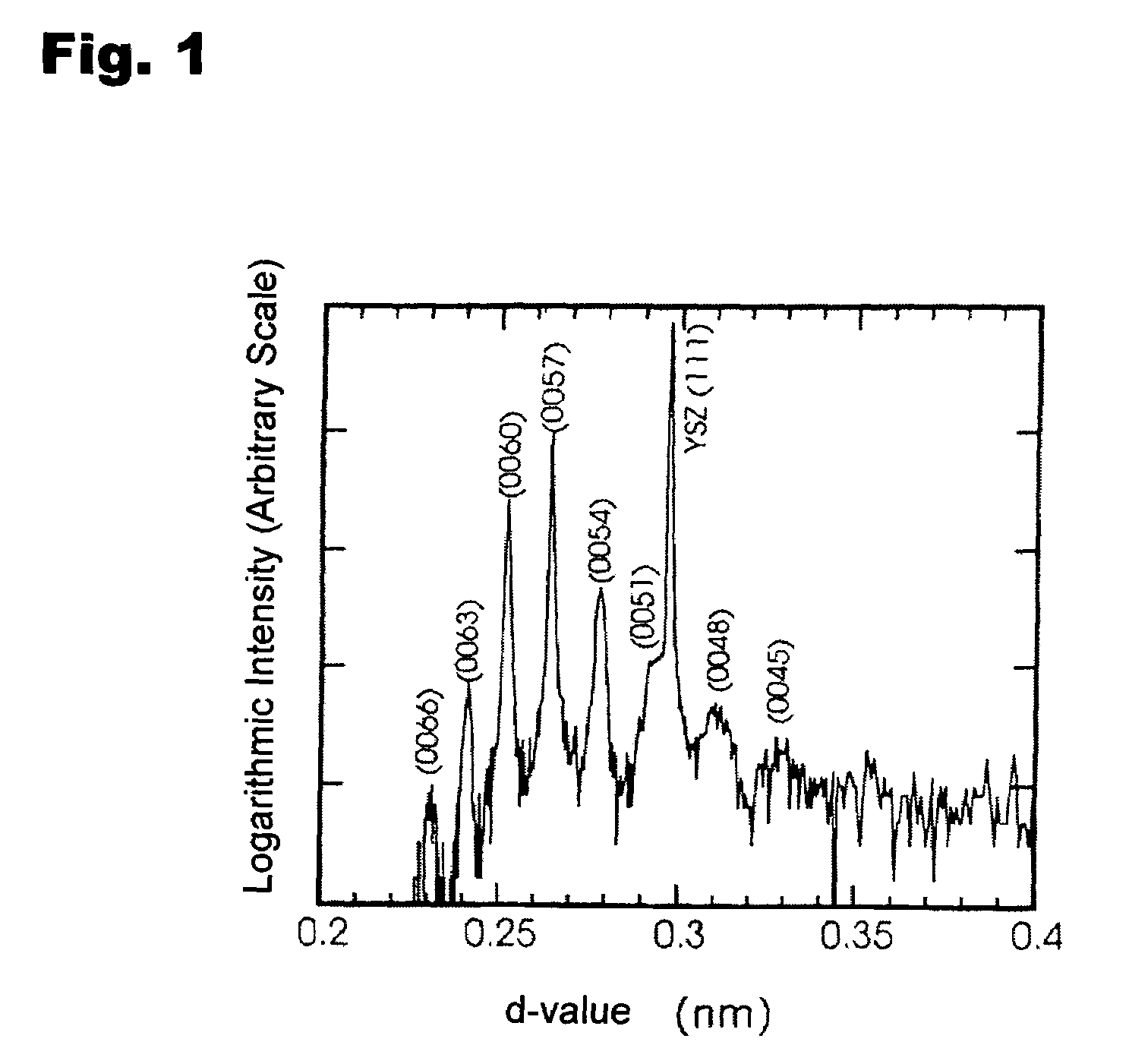
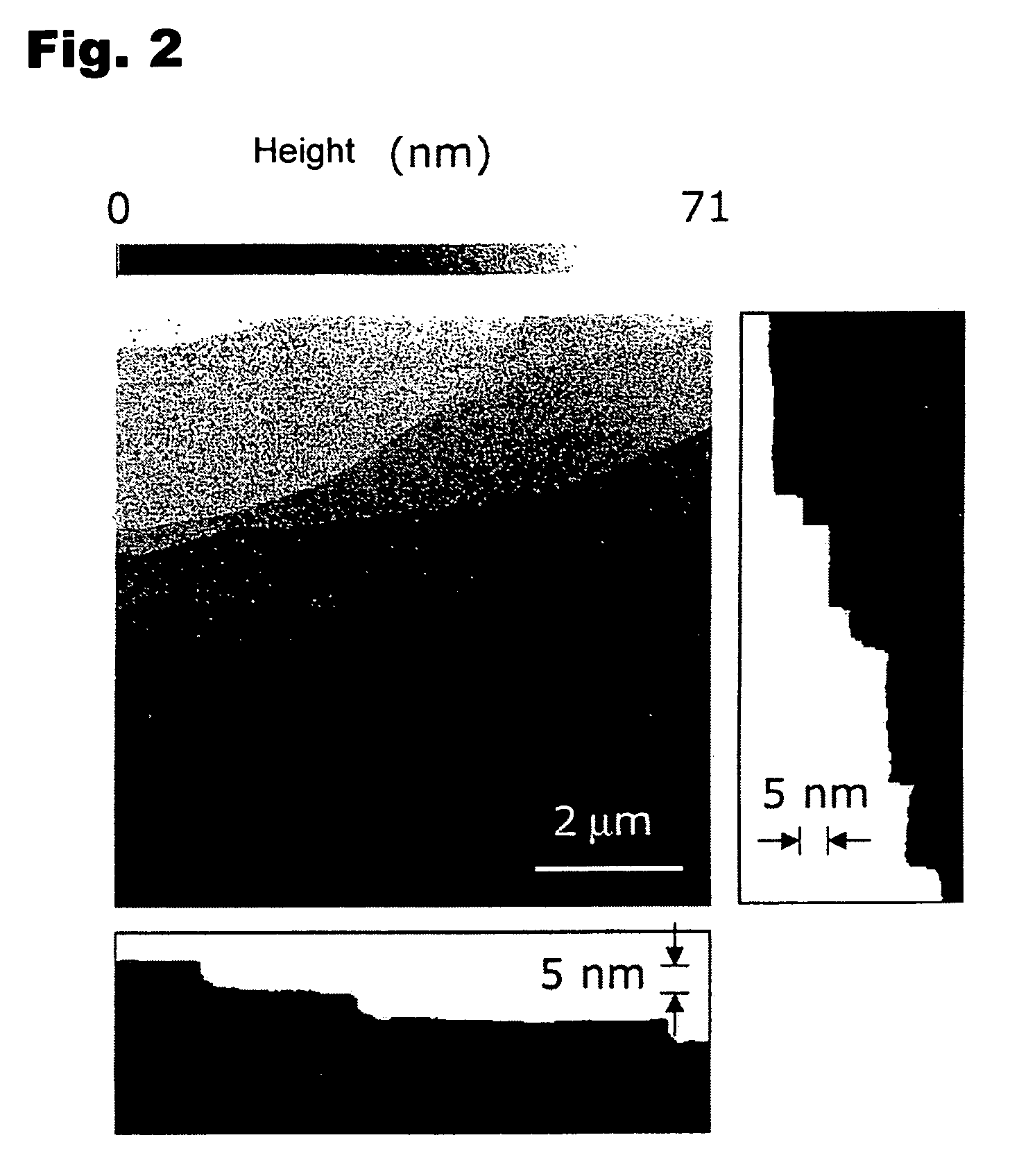
[0106]As the result of an XRD measurement, it was proved that the thin film subjected to the heating was a single crystal InGaO3 (ZnO)5 as shown in FIG. 6. Further, as the result of an AFM observation, it was proved that the surface of the thin film was an atomically smooth surface having atomical...


PUM

PropertyMeasurementUnit
smoothnessaaaaaaaaaa
thicknessaaaaaaaaaa
thicknessaaaaaaaaaa

Abstract

Disclosed is a natural-superlattice homologous single-crystal thin film, which includes a complex oxide which is epitaxially grown on either one of a ZnO epitaxial thin film formed on a single-crystal substrate, the single-crystal substrate after disappearance of the ZnO epitaxial thin film and a ZnO single crystal. The complex oxide is expressed by the formula: M1M2O3 (ZnO)m, wherein M1 is at least one selected from the group consisting of Ga, Fe, Sc, In, Lu, Yb, Tm, Er, Ho and Y, M2 is at least one selected from the group consisting of Mn, Fe, Ga, In and Al, and m is a natural number of 1 or more. A natural-superlattice homologous single-crystal thin film formed by depositing the complex oxide and subjecting the obtained layered film to a thermal anneal treatment can be used in optimal devices, electronic devices and X-ray optical devices.

Description

TECHNICAL FIELD[0001]The present invention relates to a ZnO-based complex-oxide epitaxial single-crystal thin film having a natural superlattice structure, a production method of the single-crystal thin film, and a device, such as optical devices, electronic devices and X-ray optical devices, using the single-crystal thin film.BACKGROUND ART[0002]The term “superlattice” generically means a structure formed by orderly superimposing a number of ultra-thin crystal layers consisting of different materials. The superlattice includes a “natural superlattice” based on periodicity in material's own crystal structure, and an “artificial superlattice” artificially created by alternately laminating ultra-thin films of different compositions. In case where the crystalline period or the thickness of each of the thin-film layers is in the nanometer range, periodic crystal layers or thin-film layers different in chemical composition and / or layer thickness can be variously combined to obtain specif...

Claims


Application Information

Patent Timeline
Patent Type & Authority Patents(United States)
IPC IPC(8): H01L29/10H01L29/12C30B23/02H01L21/336H01L29/45H01L29/49H01L29/786
CPCC30B23/02H01L29/45H01L29/4908H01L29/7869C30B29/22H01L29/66969C30B29/68H01L29/78693
Inventor HOSONO, HIDEOOTA, HIROMICHIORITA, MASAHIROUEDA, KAZUSHIGEHIRANO, MASAHIROKAMIYA, TOSHIO
Owner HOYA CORP
Why Eureka
Try Eureka