Amorphous oxide and field effect transistor

a field effect transistor and amorphous oxide technology, applied in the field of amorphous oxide, can solve the problems that the transistor employing silicon thin film cannot be directly formed on a less heat-resistant resin substrate, and the performance of tfts using conventional oxide semiconductor thin films is not on the same level as that of tfts using silicon, and achieve excellent properties

Active Publication Date: 2006-05-25
CANON KK +2
View PDF24 Cites 4267 Cited by
  • Summary
  • Abstract
  • Description
  • Claims
  • Application Information

AI Technical Summary

Benefits of technology

[0044] As the results of investigation on the oxide semiconductors by the inventors of the present invention, it was found that the above-mentioned ZnO is formed in a state of a polycrystalline phase, causing scattering of carriers at the interface between the polycrystalline grains to lower the electron mobility. Further it was found that ZnO is liable to cause oxygen defect therein to produce many carrier electrons, which makes difficult to lower the electrical conductivity. Thereby, even when a gate voltage is not applied to the transistor, a large electric current flow is caused between the source terminal and the drain terminal, making impossible the normally-off state of the TFT and a larger on-off ratio of the transistor.
[0050] According to the present invention, there is provided an amorphous oxide that is suitably used in the channel layer of a transistor, for example, a TFT. The present invention also provides a field effect transistor having excellent properties.

Problems solved by technology

However, the transistor employing the silicon thin film cannot by directly formed on a less heat-resistant resin substrate, since the production of the silicon thin film transistor requires a relatively high-temperature in the process,
However, TFTs using conventional oxide semiconductor thin films have not provided performances on the same level as of TFTs using silicon.

Method used


Image

  • Amorphous oxide and field effect transistor
  • Amorphous oxide and field effect transistor
  • Amorphous oxide and field effect transistor

Examples


first embodiment

Amorphous Oxide Having a Microcrystals

[0060] The invention according to the first embodiment relates to an amorphous oxide, characterized in that the amorphous contains a microcrystal(s). Where a microcrystal(s) are contained or not in the amorphous oxide is determined by taking a TEM (transmission electron microscopic) photograph of a section of a formed amorphous oxide film. An amorphous oxide film according to the present invention comprises In—Ga—Zn—O and the composition of the amorphous oxide film in a crystalline state is represented by InGaO3(ZnO)m (m is a natural number of less than 6).

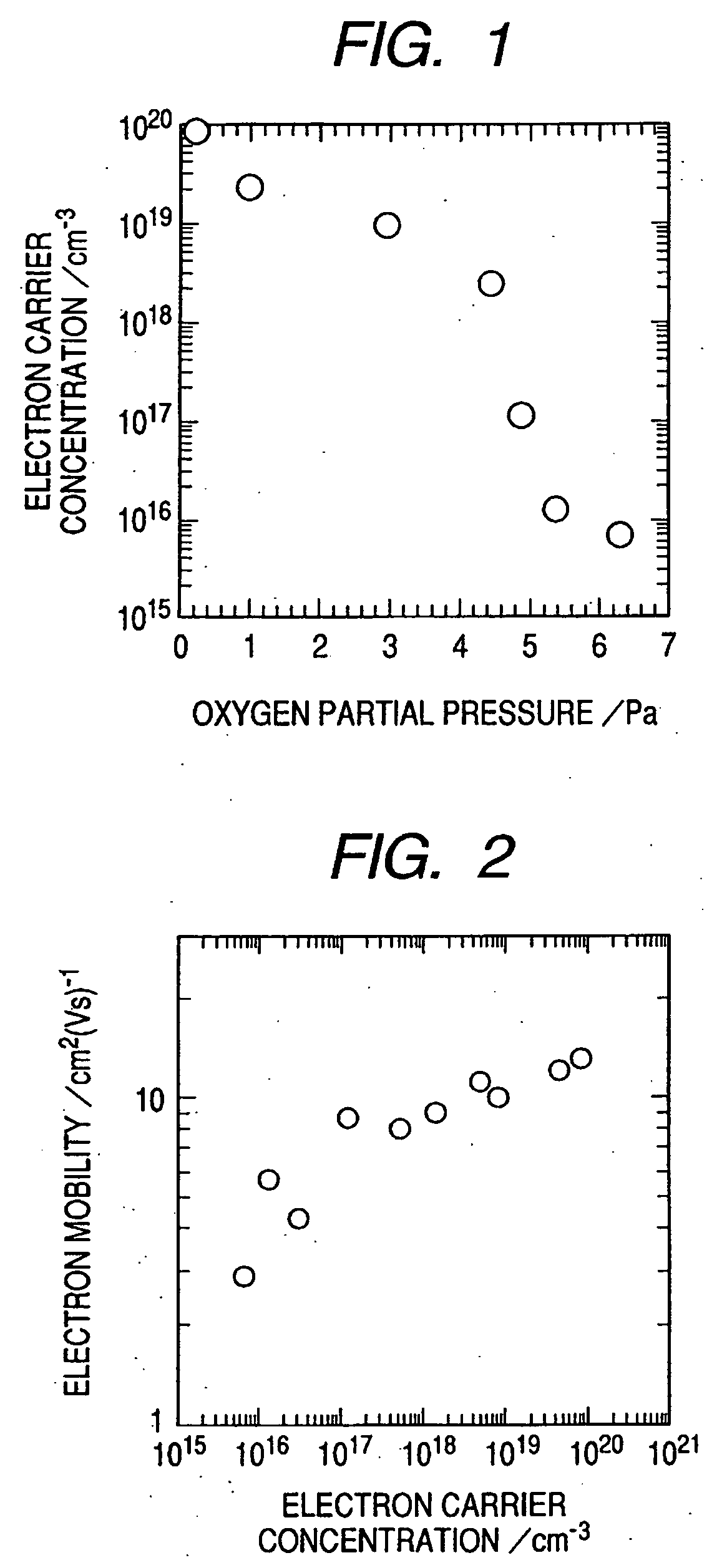
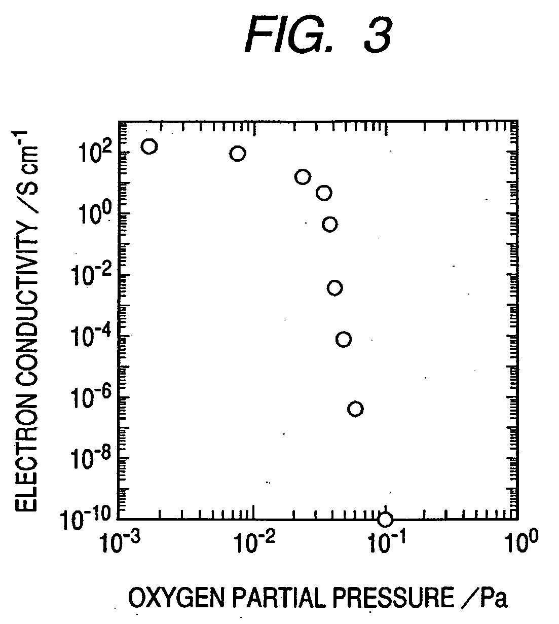
[0061] Oxides represented by the term “amorphous oxide” in the specification has an electron carrier concentration is less than 1018 / cm3 or shows a tendency that the electron mobility increases as the electron carrier concentration increases, or and so forth. Although depending on the kind of use of a TFT, it is preferable to use the amorphous TFT for fabricating normally off type TFT.

[0062...

second embodiment

Compositional Distribution of Amorphous Oxide

[0080] According to this embodiment, an amorphous oxide is characterized by a composition varying in a film-thickness direction.

[0081] The phrase “composition varying in a film-thickness direction” means that the oxygen amount contained in an oxide changes in the film thickness direction and elements constituting an oxide changes in the middle (that is, the composition changes), and the contents of the elements constituting an oxide change.

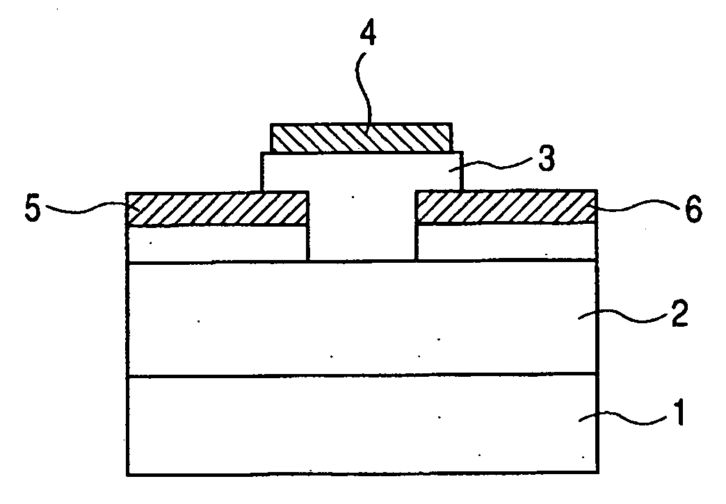
[0082] Therefore, when the amorphous oxide is used as the active layer (also called channel layer) of a field effect transistor, for example, the following constitution is preferable. In a transistor having an active layer containing an amorphous oxide and a gate insulator in contact with each other at an interface, the amorphous oxide layer is constituted such that the concentration of oxygen near the interface is set higher than the region away from the interface. In this case, since the electric r...

third embodiment

Amorphous Oxide Containing an Additive(s)

[0103] An amorphous oxide according to this embodiment is characterized in that the amorphous oxide contains at least one or plurality of types of elements selected from the group consisting of Li, Na, Mn, Ni, Pd, Cu, Cd, C, N, P, Ti, Zr, V, Ru, Ge, Sn, and F are contained as an additive. Introduction of an additive into an amorphous oxide is attained by introducing the additive in a gas for use in a film formation apparatus or in the film formation apparatus, or in a target material that is used in the apparatus. As a matter of course, after a film is formed from an amorphous oxide without an additive, the additive may be introduced into the film as is described later in Examples.

[0104] The electron carrier concentration of the amorphos oxide is preferably less than 1018 / cm3.

[0105] An amorphous oxide according to the present invention may include a transparent amorphous oxide comprising In—Ga—Zn—O and whose composition in a crystalline st...


PUM


Abstract

A novel amorphous oxide applicable, for example, to an active layer of a TFT is provided. The amorphous oxide comprises microcrystals.

Description

BACKGROUND OF THE INVENTION [0001] 1. Field of the Invention [0002] The present invention relates to an amorphous oxide. The present invention also relates to a field effect transistor using an amorphous oxide. [0003] 2. Related Background Art [0004] In recent years, flat panel display (FPD) is commercialized as the results of progress of liquid crystal techniques, electroluminescence (EL), and the related techniques. The FPD is driven by an active matrix circuit comprising a field-effect thin film transistor (TFT) employing an amorphous silicon thin film or polycrystalline silicon thin film as the active layer formed on a glass substrate. [0005] For smaller thickness, lighter weight, and higher impact strength of the FPD, use of a lightweight and a flexible resin substrate is investigated in place of the glass substrate. However, the transistor employing the silicon thin film cannot by directly formed on a less heat-resistant resin substrate, since the production of the silicon thi...

Claims


Application Information

Patent Timeline
Patent Type & Authority Applications(United States)
IPC IPC(8): H01L27/12
CPCH01L21/428H01L29/7869H01L29/78693H01L21/02422H01L29/78696H01L21/02565H01L21/02592H01L21/02631H01L21/02554H01L29/66969H01L29/26H01L29/06H01L27/1225H01L27/124
Inventor SANO, MASAFUMINAKAGAWA, KATSUMIHOSONO, HIDEOKAMIYA, TOSHIONOMURA, KENJI
Owner CANON KK
Why Eureka
Try Eureka