

Electric elements and circuits utilizing amorphous oxides
a technology of amorphous oxides and electric elements, applied in the direction of basic electric elements, electrical apparatus, semiconductor devices, etc., can solve the problem of difficult to form directly onto a resin substrate having low heat resistan
- Summary
- Abstract
- Description
- Claims
- Application Information
AI Technical Summary
Benefits of technology
Problems solved by technology
Method used
Image

Examples
first embodiment
Semiconductor Device
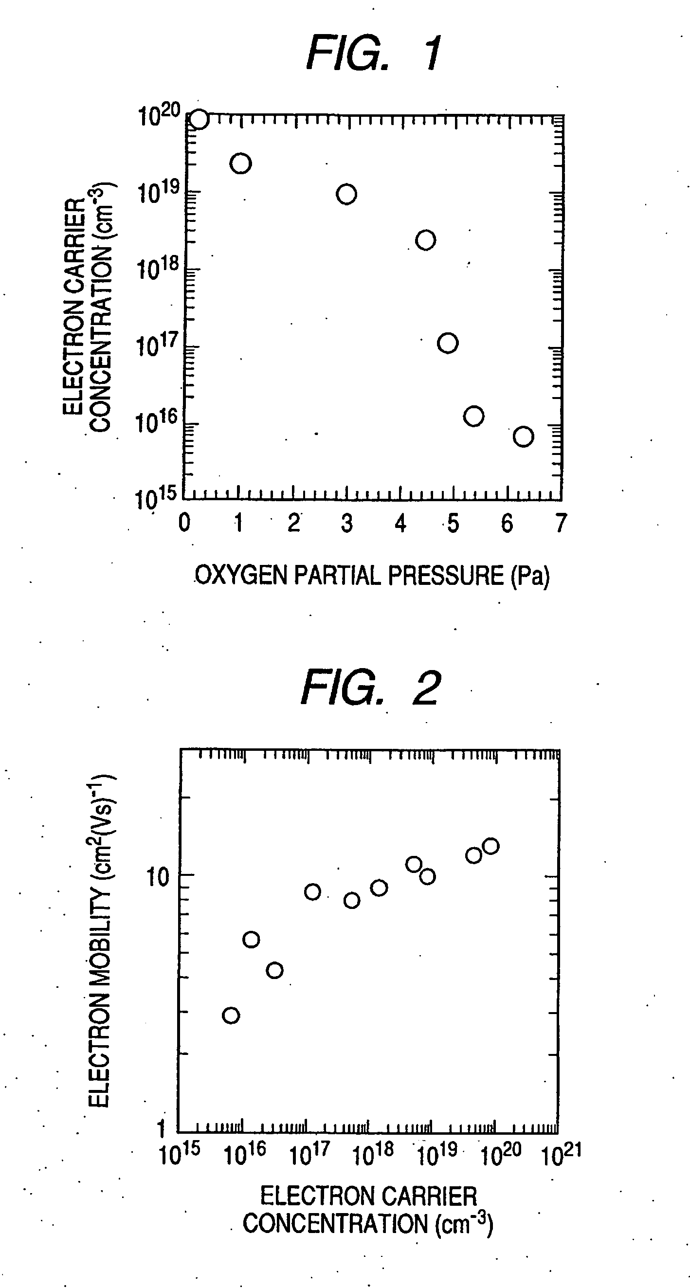
[0102] Firstly, a semiconductor device having a P-type region and an N-type region will be described. Here, the semiconductor device of concern contains PN-junction transistors and heterojunction devices. The present invention is featured by use as amorphous oxides configuring an N-type region of oxides with electron carrier concentration less than 1×10¹⁸ / cm3 or oxides, or oxides showing tendency of increase in electron mobility as electron carrier concentration increases. These amorphous oxides will be described later. Here, on a substrate, either provision of the N-type region inside the P-type region or provision of the P-type region inside the N-type region is also a preferable mode. In addition, forming of the P-type region and the N-type region in the same layer on a substrate is also a preferable mode. In addition, configuration of the P-type region and the N-type region made from different amorphous oxides materials is also a preferable mode. Moreover, t...
second embodiment
[0128] In addition, the present invention relates to a logic circuit with TFT including the transparent being semiconductor film, use as N-TFT.
[0129] In particular, N-TFT with use of a resistance with the transparent film being electronic conductor and the transparent film is connected in series between the power supply and the ground potential (GND) taking the gate of the N-TFT as signal input and the source of the TFT as output.
[0130] Thereby, an inverter circuit using the transparent film as a semiconductor layer can be configured.
[0131] Moreover, using P-type TFT (hereinafter to be referred to as P-TFT) with use of P-type semiconductor as an active layer instead of the resistance, and taking the gate of P-TFT as the input common with the gate of N-TFT, a complementary TFT circuit can be configured.
[0132] This derives an effect that the pass-through current at the time of operation of an inverter is restrained to enable configuration of a circuit with low p...
example 1
SIT Element with Use of the Transparent Film
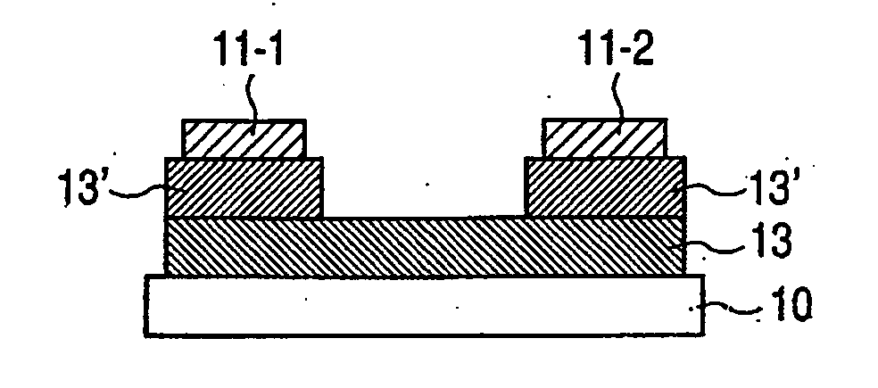
[0287] As shown in FIG. 7, an ITO thin film of 30 nm is formed with pulsed laser deposition on an insulating substrate 10 made of such as glass and plastic etc., and the drain electrode 11-1 undergoes patterning with a photolithography method and a liftoff method. Subsequently, an In—Ga—Zn—O system amorphous N-type semiconductor 13 of 30 nm is formed with pulsed laser deposition, and the In—Ga—Zn—O system amorphous N-type semiconductor film is formed with a photolithography method and a liftoff method on the electrode 11-1. Thereafter, as an electrode 12, Pt thin film of 30 nm is formed with pulse laser deposition and undergoes patterning with a photolithography method and a liftoff method on the semiconductor film so as to resemble the teeth of a comb. Moreover, the In—Ga—Zn—O system amorphous N-type semiconductor 13 of 30 nm is formed with pulsed laser deposition, and the In—Ga—Zn—O system amorphous N-type semiconductor undergoes patter...
PUM
 Abstract
Description
Claims
Application Information