Semiconductor device and method for producing the same

a technology of semiconductor devices and semiconductors, applied in the direction of semiconductor devices, electrical devices, transistors, etc., can solve the problems of not being able to obtain desirable transistor characteristics, and achieve the effects of reducing ion density, and reducing plasma doping pressur

Active Publication Date: 2009-11-26
GK BRIDGE 1
View PDF25 Cites 383 Cited by
  • Summary
  • Abstract
  • Description
  • Claims
  • Application Information

AI Technical Summary

Benefits of technology

[0052](4) the factor that etches the corner portion (the upper corner) of a fin-shaped semiconductor region is basically the ions in the plasma, and the amount of etching of the corner portion is suppressed by reducing the ion density.
[0053]Based on these findings, the primary characteristic of the method for producing a semiconductor device of the present invention lies in “decreasing the pressure during plasma doping as the mass of the introduced impurity increases” Thus, by sufficiently decreasing the pressure during plasma doping, the ion density decreases to a very low level, thereby suppressing the amount of etching of the corner portion of the fin-shaped semiconductor region. At the same time, it is possible to reduce the amount of impurity incident upon the principle plane of the substrate in a perpendicular direction, and to relatively increase the amount of impurity incident upon the principle plane of the substrate in random directions. Moreover, for the decrease in the implantation dose due to the decrease in the ion density, it is possible to compensate for the decrease in the implantation dose to thereby achieve a desirable implantation dose by increasing the proportion of an impurity-containing gas in the material gas with respect to the diluent gas. Therefore, it is possible to obtain a semiconductor device in which an impurity region in a side portion of the semiconductor region has an implantation dose of 80% or more of that in an upper portion of the semiconductor region. Therefore, it is possible to obtain desirable transistor characteristics even if the proportion of the width of the impurity region formed in the side portion of the fin-shaped semiconductor region increases with respect to the width in the gate width direction of the extension region and the source-drain region of a fin-shaped FET, for example.

Problems solved by technology

However, with conventional methods for producing a semiconductor device disclosed in documents such as Patent Document 1 and Non-Patent Document 1 identified above, it is not possible to obtain desirable transistor characteristics.

Method used


Image

  • Semiconductor device and method for producing the same
  • Semiconductor device and method for producing the same
  • Semiconductor device and method for producing the same

Examples


first example

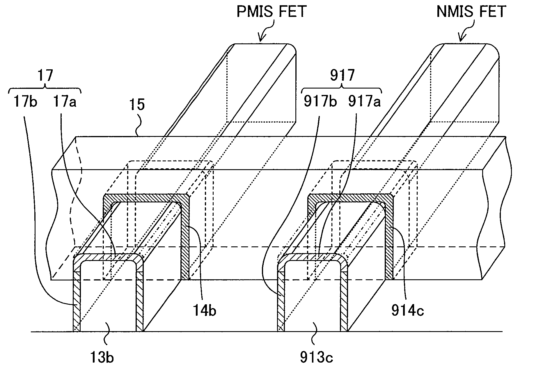
[0139]FIG. 5A is a perspective view of an example (first example) of a fin-shaped CMISFET, and FIG. 5B is an enlarged perspective view showing an NMISFET of the fin-shaped CMISFET shown in FIG. 5A. In FIGS. 5A and 5B, like elements to those of the fin-shaped CMISFET shown in FIGS. 1A-1E are denoted by like reference numerals and will not be described redundantly.

[0140]First, referring to FIG. 5B, the chipping of the fin corner portion (the upper corner) of a fin-shaped NMISFET will be described. This similarly applies to the chipping of the fin corner portion of a fin-shaped PMISFET. As shown in FIG. 5B, the gate electrode 15c is formed so as to extend across the p-type fin-shaped semiconductor region 913c having the n-type impurity region 917a in an upper portion thereof and the n-type impurity region 917b in a side portion thereof, with the gate insulating film 914c interposed therebetween. Herein, the height and the width of the p-type fin-shaped semiconductor region 913c (and th...

second example

[0197]FIG. 20A is a perspective view of another example (second example) of a fin-shaped CMISFET, and FIG. 20B is an enlarged perspective view showing an NMISFET of the fin-shaped CMISFET shown in FIG. 20A. In FIGS. 20A and 20B, like elements to those of the fin-shaped CMISFET shown in FIGS. 1A-1E are denoted by like reference numerals and will not be described redundantly.

[0198]First, referring to FIG. 20B, the chipping of the fin corner portion (the upper corner) of a fin-shaped NMISFET, and the specific resistance of the n-type impurity region in the fin upper portion and that of the n-type impurity region in the fin side portion will be described. They similarly apply to a fin-shaped PMISFET. While “specific resistance (resistivity)” is mainly used in the following description, the magnitude of the resistance can be represented by “sheet resistance” or “spreading resistance” instead of “specific resistance”. As shown in FIG. 20B, the gate electrode 15c is formed so as to extend ...

first embodiment

Second Variation of First Embodiment

[0224]A structure of a semiconductor device according to a second variation of the first embodiment (including the first example and the second example) will now be described with reference to the drawings.

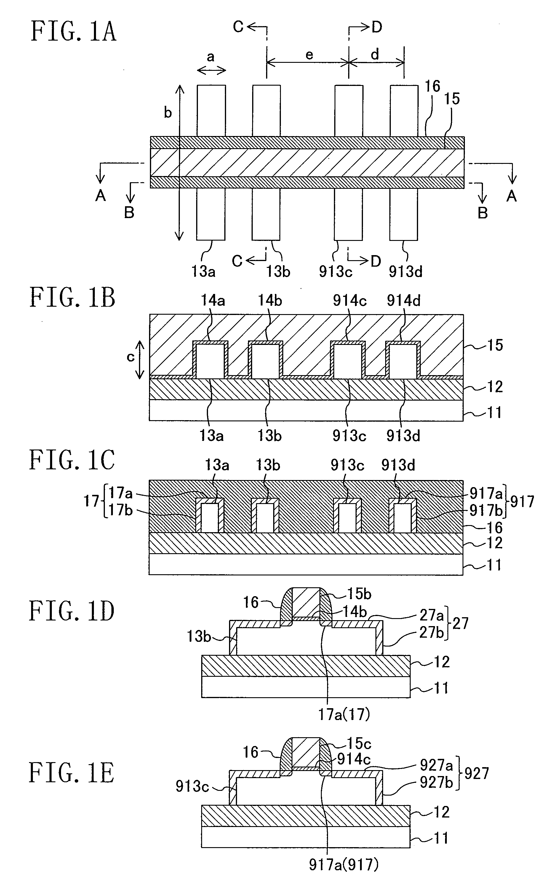
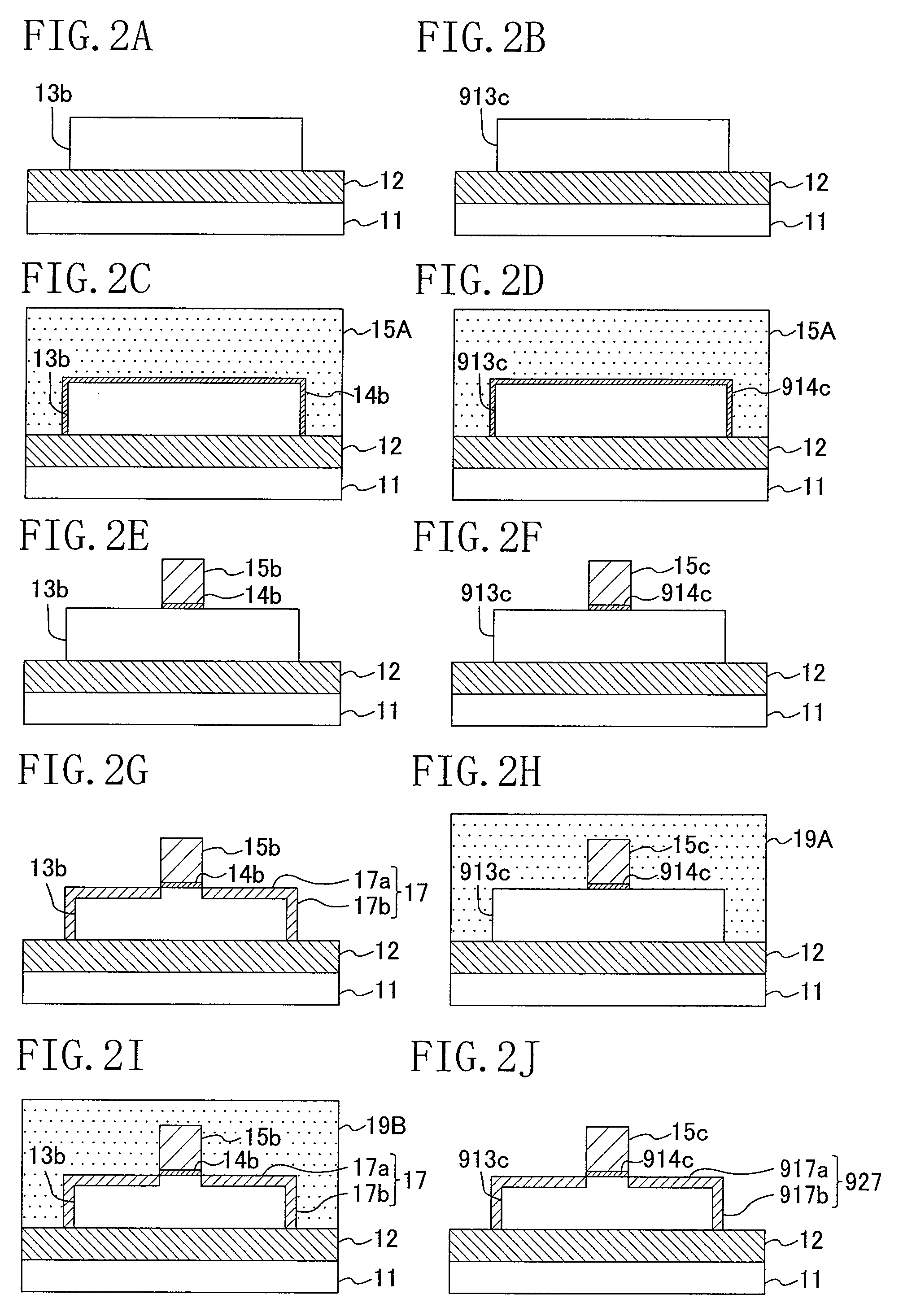
[0225]A plan view showing a structure of a semiconductor device of this variation, specifically, a semiconductor device including a fin-shaped CMISFET, is the same as FIG. 1A being a plan view of the first embodiment. FIGS. 25A-25D show cross-sectional structures of the semiconductor device of this variation, wherein FIG. 25A is a cross-sectional view taken along line A-A in FIG. 1A, FIG. 25B is a cross-sectional view taken along line B-B in FIG. 1A, FIG. 25C is a cross-sectional view taken along line C-C in FIG. 1A, and FIG. 25D is a cross-sectional view taken along line D-D in FIG. 1A.

[0226]As shown in FIGS. 25A-25D, this variation differs from the first embodiment shown in FIGS. 1A-1E as follows. That is, in the first embodiment, the gate ins...


PUM


Abstract

First and second gate insulating films are formed so as to cover at least the upper corner of first and second fin-shaped semiconductor regions. The radius of curvature r1′ of the upper corner of the first fin-shaped semiconductor region located outside the first gate insulating film is greater than the radius of curvature r1 of the upper corner of the first fin-shaped semiconductor region located under the first gate insulating film and is less than or equal to 2×r1. The radius of curvature r2′ of the upper corner of the second fin-shaped semiconductor region located outside the second gate insulating film is greater than the radius of curvature r2 of the upper corner of the second fin-shaped semiconductor region located under the second gate insulating film and is less than or equal to 2×r2.

Description

CROSS REFERENCE TO RELATED APPLICATIONS[0001]This is a continuation-in-part of U.S. patent application Ser. No. 12 / 193,861, filed on Aug. 19, 2008, which is a continuation of International Application No. PCT / JP2008 / 000303, filed on Feb. 22, 2008, which claims priority to Japanese Patent Application No. 2007-195860, filed on Jul. 27, 2007. This application claims priority under 35 U.S.C. §119(a) to Japanese Patent Applications No. 2007-195860, and No. 2008-198477, filed on Jul. 31, 2008. The entire contents of these applications is herein incorporated by reference in their entirety.BACKGROUND OF THE INVENTION[0002]The present disclosure relates to a semiconductor device and a method for producing the same, and more particularly to a semiconductor device of a three-dimensional structure including fin-shaped semiconductor regions on a substrate and a method for producing the same.[0003]In recent years, demands for miniaturizing semiconductor devices have been increasing along with the...

Claims


Application Information

Patent Timeline
Patent Type & Authority Applications(United States)
IPC IPC(8): H01L29/78H01L27/092H01L21/8238
CPCH01L29/66795H01L29/7854H01L29/66803
Inventor SASAKI, YUICHIRONAKAMOTO, KEIICHIOKASHITA, KATSUMIKANADA, HISATAKAMIZUNO, BUNJI
Owner GK BRIDGE 1
Why Eureka
Try Eureka