Oxide semiconductor thin film transistor and method of manufacturing the same

a thin film transistor and semiconductor technology, applied in the field of thin film transistors, can solve the problems of difficult manufacturing of normally-off tft, achieve the effects of preventing unstable operation, reducing the unstability of tft characteristics caused by the change of atmosphere, and stable tft operational characteristics

Inactive Publication Date: 2007-03-08
CANON KK
View PDF6 Cites 4121 Cited by
  • Summary
  • Abstract
  • Description
  • Claims
  • Application Information

AI Technical Summary

Benefits of technology

[0007] Therefore, an object of the present invention is to provide a device with high reliability and reduced unstability of TFT characteristics which is caused by a change in atmosphere, in a TFT in which the oxide semiconductor containing In, M, Zn, and O, where M represents at least one of Ga, Al, and Fe, is used for the channel layer, unstability of TFT characteristics which is caused by a change in atmosphere.
[0009] According to the present invention, in a normally-on TFT in which an oxide semiconductor containing In, M, Zn, and O, where M represents at least one of Ga, Al, and Fe, such as a transparent oxide thin film, is used for the channel layer, covering the channel layer with a protective film prevents an unstable operation caused by the change in atmosphere. Therefore, stable TFT operational characteristics are obtained. Thus, the unstability of TFT characteristics which is caused by the change in atmosphere can be reduced to provide a device having high performance, stability, and reliability.

Problems solved by technology

However, when a ZnO thin film is used for the channel layer, there is such a disadvantage that it is difficult to manufacture a normally-off TFT.

Method used


Image

  • Oxide semiconductor thin film transistor and method of manufacturing the same
  • Oxide semiconductor thin film transistor and method of manufacturing the same
  • Oxide semiconductor thin film transistor and method of manufacturing the same

Examples


first embodiment

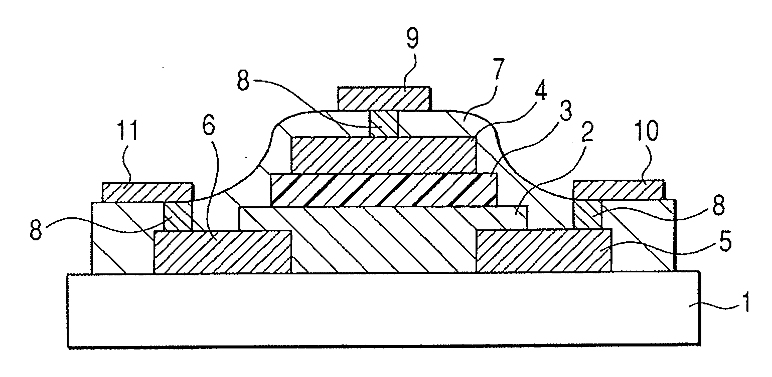
[0026] The structure of a TFT device including a thin film transistor according to a first embodiment of the present invention will be described.

[0027] The TFT device is a three-terminal device including a gate terminal, a source terminal, and a drain terminal. A semiconductor thin film formed on a dielectric substrate such as a plastic film substrate is used as a channel layer through which electrons or holes move. With this structure, the TFT device is an active device having a function of controlling a current flowing into the channel layer according to a voltage applied to the gate terminal to switch a current flowing between the source terminal and the drain terminal.

[0028] The TFT device which can be used here is, for example, a device having a stagger (top gate) structure in which a gate dielectric film and a gate terminal are formed on a semiconductor channel layer in this order or a device having an inverse stagger (bottom gate) structure in which a gate dielectric film a...

second embodiment

[0036] Next, a second embodiment of the present invention will be described. According to this embodiment, a film including at least one selected from the group consisting of a silicon nitride (SiNx), a silicon oxide (SiOx), and a silicon oxynitride (SiOxNy) can be used as the protective film formed on the TFT device.

[0037] It is preferable that a CVD method be used as a method of forming a silicon nitride film, a silicon oxide film, or a silicon carbide film as the protective film on the TFT. According to a preferable mode, an deposition method such as deposition using resistance heating, laser deposition, or electron beam deposition is used. According to another preferable mode, a sputtering method is used. Above all, the CVD method is most preferably used to form the silicon nitride film (SiNx), the silicon oxide film (SiOx), or the silicon oxynitride film (SiOxNy).

[0038] It is preferable that a temperature at which the film including at least one selected from the group consis...

third embodiment

[0044] In a third embodiment of the present invention, an organic substance film can be used as the protective film formed on the TFT device. In this case, according to a preferable mode, a polyimide film is used as the organic substance film. According to another preferable mode, a fluorinated organic substance resin film such as a silicone film is used as the organic substance film.

[0045] It is preferable that a solution applying method of applying a solution and then performing drying or heating to form a film be used as a method of forming the organic substance film as the protective film on the TFT.

[0046] Further, it is preferable that a temperature at which the organic substance film is formed as the protective film on the TFT using the above-mentioned method be equal to or lower than 200° C.

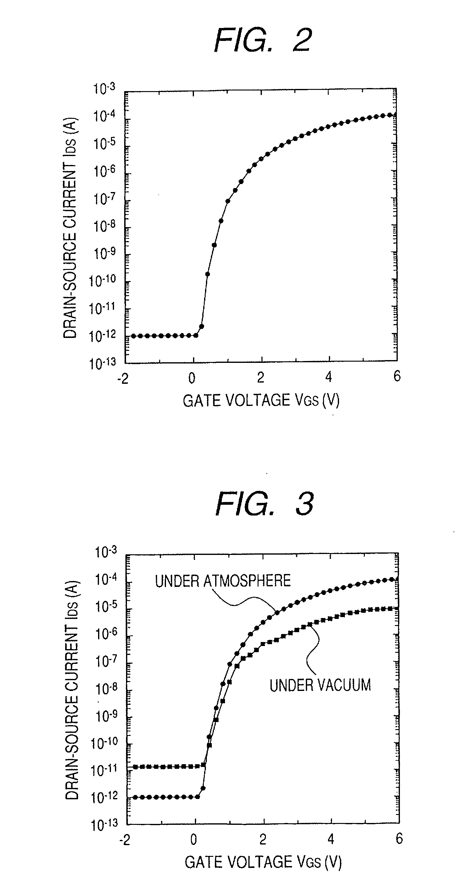
[0047] Therefore, the effect that the TFT operation is not influenced by an atmosphere and thus stable operation can be performed without causing unstable operation due to a change in a...


PUM


Abstract

Provided is a thin film transistor comprising a channel layer comprised of an oxide semiconductor containing In, M, Zn, and O, M including at least one selected from the group consisting of Ga, Al, and Fe. The channel layer is covered with a protective film.

Description

BACKGROUND OF THE INVENTION [0001] 1. Field of the Invention [0002] The present invention relates to a thin film transistor (TFT) in which an oxide semiconductor containing In, M, Zn, and O, where M represents at least one of Ga, Al, and Fe, is used for a channel layer and a method of manufacturing the thin film transistor. [0003] 2. Description of the Related Art [0004] In recent years, there is an attempt to form a transparent film as a channel layer of a transistor using a conductive oxide thin film. For example, a TFT in which a polycrystalline thin film of a transparent conductive oxide containing ZnO as a main ingredient is used for the channel layer is under active development (see JP 2002-076356 A) The thin film can be formed at low temperatures and is transparent to visible light, so it is assumed that a flexible transparent TFT can be formed on a substrate such as a plastic plate or a film. [0005] However, when a ZnO thin film is used for the channel layer, there is such a...

Claims


Application Information

Patent Timeline
Patent Type & Authority Applications(United States)
IPC IPC(8): H01L27/12
CPCH01L29/7869
Inventor YABUTA, HISATO
Owner CANON KK
Why Eureka
Try Eureka