Field effect transistor

a field effect transistor and transistor technology, applied in the field of field effect transistors, can solve the problems that the transistor using silicon thin film cannot be directly formed on a less heat-resistant resin substrate, and the transistor has not been obtained which satisfies

Active Publication Date: 2006-06-01
CANON KK +2
View PDF13 Cites 4116 Cited by
  • Summary
  • Abstract
  • Description
  • Claims
  • Application Information

AI Technical Summary

Benefits of technology

[0008] The present invention intends to provide a novel field effect transistor employing an amorphous oxide.

Problems solved by technology

However, the transistor employing the silicon thin film cannot by directly formed on a less heat-resistant resin substrate, since the production of the silicon thin film transistor requires a relatively high-temperature in the process.
However, a transistor has not been obtained which satisfies simultaneously all of the properties of transparency and electric properties of the TFT, properties of the gate-insulating film, prevention of current leakage, and adhesiveness between the active layer and the substrate.

Method used


Image

  • Field effect transistor
  • Field effect transistor
  • Field effect transistor

Examples


first embodiment

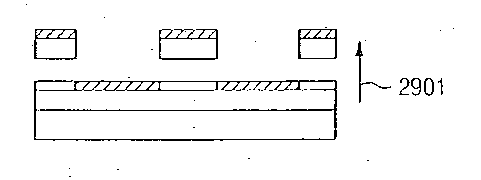
Transparent S,D,G Electrodes or Laminated Electrodes

[0080] The field-effect transistor of this embodiment belongs to the category of the aforementioned first, second, and third aspects of the invention.

[0081] The description “transparent to visible light” signifies a state in which the material is transparent to at least a part of the visible light wavelength region. The transparency signifies a state of not only no light absorption but also penetration of a part of the visible light. In the present invention, the transmittance of visible light is not lower than 40%, more preferably not lower than 60%, still more preferably not lower than 80%.

[0082] Thus, a highly transparent device is realized by making transparent at least a portion of the electrode or another member constituting the transistor.

[0083] Desirably, all of the source electrode, the drain electrode, the gate electrode, and the gate-insulating film are transparent to the visible light. Examples of electrodes transpa...

second embodiment

Multilayered Gate Insulator

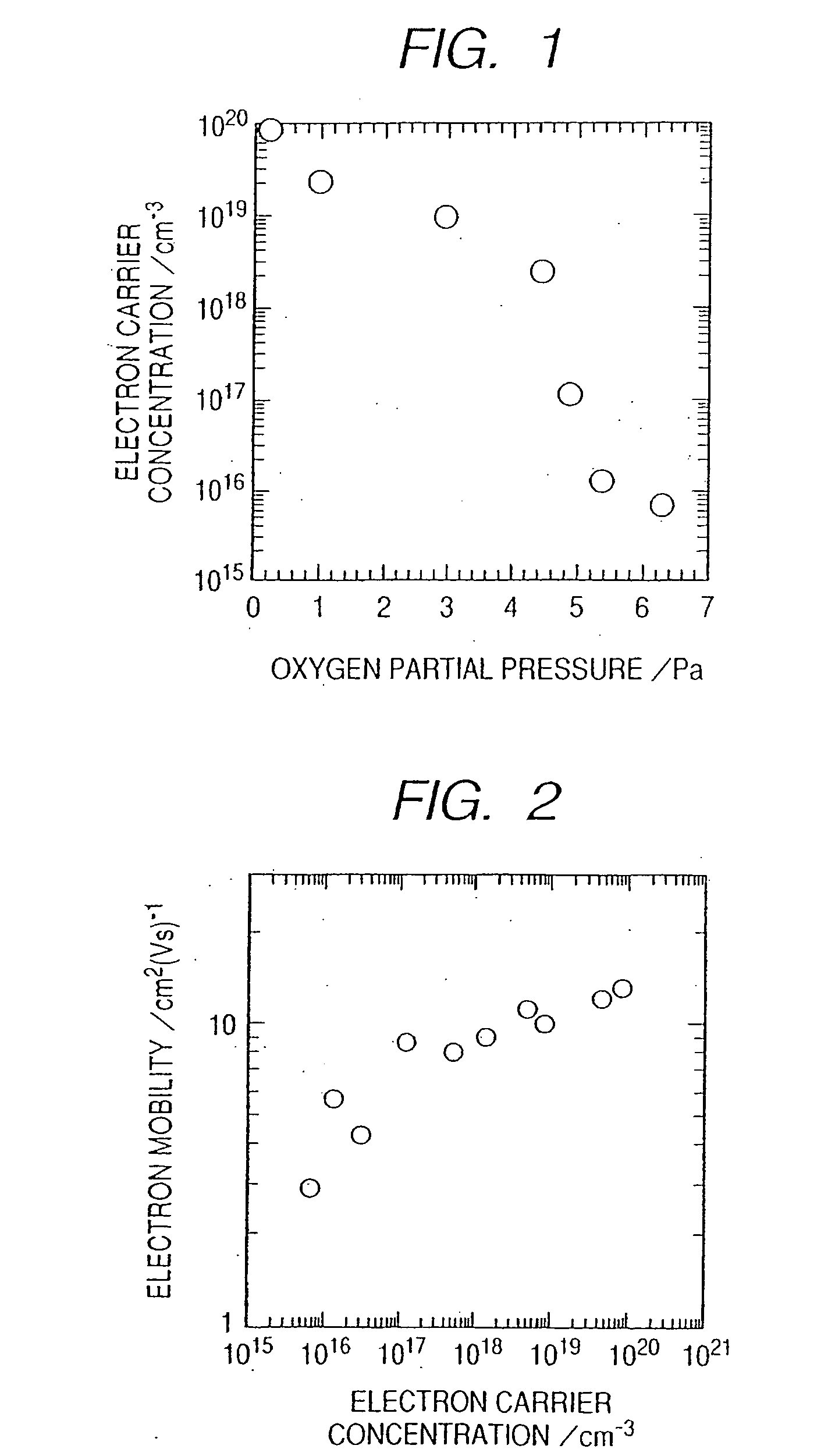
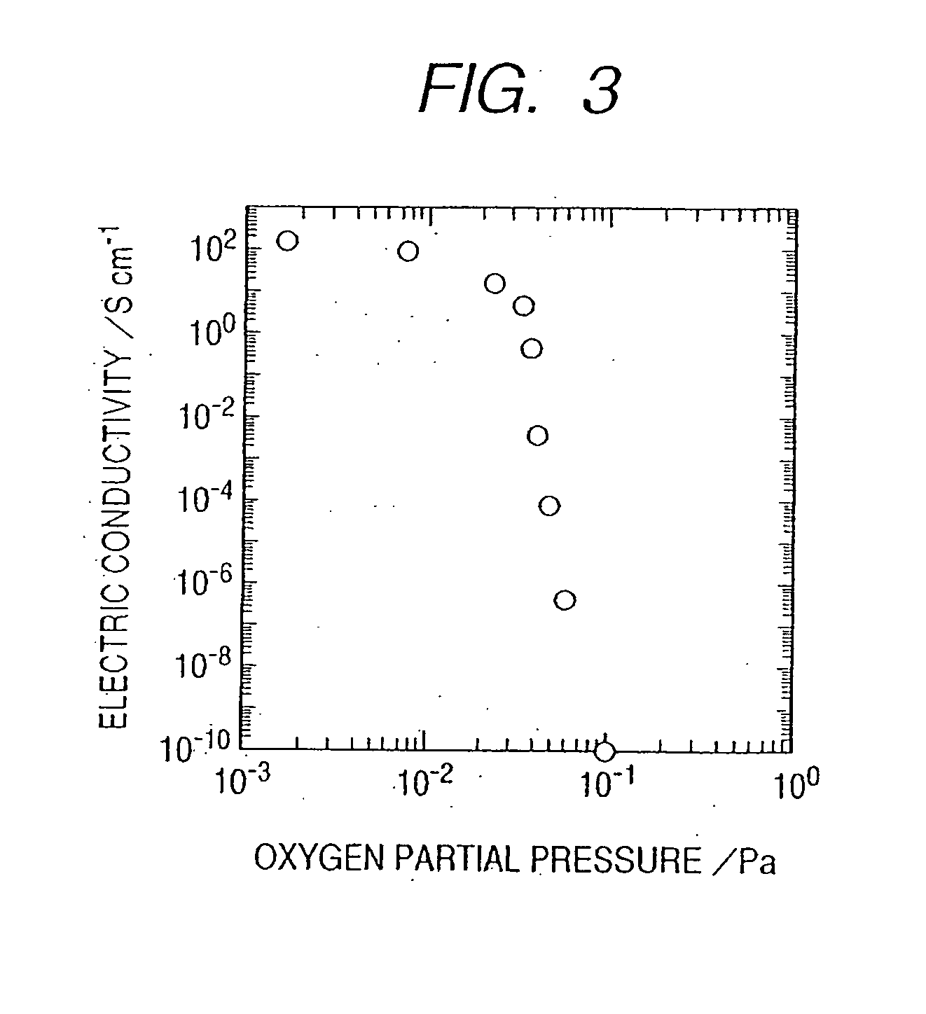
[0088] The field effect transistor of this embodiment belongs to the category of the above fourth and fifth aspects of the invention. The active Layer of this embodiment is preferably constituted of an transparent amorphous oxide containing at least In—Ga—Zn—O, represented by InGaO3(ZnO)m (m: a natural number of less than 6) in a crystal state, containing carriers at a concentration of less than 1×10¹⁸ / cm3; or a transparent amorphous oxide containing In—Ga—Zn—Mg—O, represented by InGaO3(Zn1−xMgxO)n (m: a natural number of less than 6; 0

[0089] The first layer constituting the gate-insulating film is constituted of, for example, HfO2′ or Y2O3, or a mixed crystal compound thereof. The second layer is constituted, for example, of SiO2, Si3N4, TiO2, Ta2O5, PbTiO3, BaTa2O6, SrTiO3, MgO, or AlN, or an amorphous structure containing the above substance.

[0090] The above materials of the first layer and the second layer are examples, and ...

third embodiment

Passivation, Surface-Coating Layer

[0121] The field-effect transistor of this embodiment belongs to the category of the above seventh, eighth and ninth aspects of the invention.

[0122] The passivation layer in the fifth aspect includes two conceptions. The passivation layer of a first conception is a separate layer provided between the active layer and the gate-insulating layer and constituted of a material different from that of the active layer or the gate-insulating layer. This passivation layer of the first concept is hereinafter referred to a “passivated layer”. The passivated layer is composed, for example, of amorphous silicon oxide, amorphous silicon nitride, titanium oxide, aluminum oxide, magnesium oxide, or the like.

[0123] The passivation layer of a second conception is an outermost surface portion of the active layer treated with oxygen plasma. The treatment for formation of the passivation layer of the second conception is hereinafter referred to as “passivation treatm...


PUM


Abstract

A novel field-effect transistor is provided which employs an amorphous oxide. In an embodiment of the present invention, the transistor comprises an amorphous oxide layer containing electron carrier at a concentration less than 1×10⁻¹⁸/cm3, and the gate-insulating layer is comprised of a first layer being in contact with the amorphous oxide and a second layer different from the first layer.

Description

BACKGROUND OF THE INVENTION [0001] 1. Field of the Invention [0002] The present invention relates to a field effect transistor employing an amorphous oxide. [0003] 2. Related Background Art [0004] In recent years, flat panel display (FPD) is commercialized as the results of progress of liquid crystal techniques, electroluminescence (EL), and the related techniques. The FPD is driven by an active matrix circuit comprising a field-effect thin film transistor (TFT) employing an amorphous silicon thin film or polycrystalline silicon thin film as the active layer formed on a glass substrate. [0005] For smaller thickness, lighter weight, and higher impact strength of the FPD, use of a lightweight and a flexible resin substrate is investigated in place of the glass substrate. However, the transistor employing the silicon thin film cannot by directly formed on a less heat-resistant resin substrate, since the production of the silicon thin film transistor requires a relatively high-temperatu...

Claims


Application Information

Patent Timeline
Patent Type & Authority Applications(United States)
IPC IPC(8): H01L29/04H01L27/12H01L31/0376
CPCH01L29/51H01L29/7869H01L21/02422H01L21/02554H01L21/02565H01L21/02631H01L29/4908H01L29/66969H01L29/78693
Inventor SANO, MASAFUMINAKAGAWA, KATSUMIHOSONO, HIDEOKAMIYA, TOSHIONOMURA, KENJI
Owner CANON KK
Why Eureka
Try Eureka