Methods of making thin film transistors comprising zinc-oxide-based semiconductor materials and transistors made thereby

a technology of zinc oxide-based semiconductor materials and thin film transistors, which is applied in the direction of semiconductor devices, electrical devices, nanotechnology, etc., can solve the problems of wasting materials, amorphous silicon, and requiring relatively difficult or complicated processes,

Active Publication Date: 2008-07-22
EASTMAN KODAK CO
View PDF18 Cites 4067 Cited by
  • Summary
  • Abstract
  • Description
  • Claims
  • Application Information

AI Technical Summary

Problems solved by technology

The deposition of amorphous silicon, during the manufacture of transistors, requires relatively difficult or complicated processes such as plasma enhanced chemical vapor deposition and high temperatures (about 360° C.) to achieve the electrical characteristics sufficient for display applications.
These patterning steps are time consuming and waste materials.
Such plastics, however, limit device processing to below 200° C.
However, most organic semiconductors generally have inferior or problematic electronic properties compared to amorphous silicon for use in transistor devices.
For example, organic materials may tend to degrade in normal atmospheric conditions.
The portion of the display glass occupied by the addressing electronics is not available for transmission of light through the display.

Method used


Image

  • Methods of making thin film transistors comprising zinc-oxide-based semiconductor materials and transistors made thereby
  • Methods of making thin film transistors comprising zinc-oxide-based semiconductor materials and transistors made thereby
  • Methods of making thin film transistors comprising zinc-oxide-based semiconductor materials and transistors made thereby

Examples


example 1

[0118]This example shows that working TFT devices can be created from a nanoparticle film at low temperatures. The semiconductor coating solution was prepared by diluting the above nanoparticle formulation, NLF-1, to 1.0% in ethanol. The above solution was applied to the substrate by spin coating at a rate of 1000 or 2000 rpm. After the spin coating, the Samples 1-1 through 1-4 were annealed for 10 minutes at a range of temperatures between 50° C. and 200° C. in dry air. Subsequent sample processing is as described above. Device testing yielded the following parameters:

[0119]

TABLE 1-1ExtractedMobilitySampleSpin SpeedTemperature(cm2 / Vs)1-11000 rpm 50 C.0.0014 cm2 / Vs1-21000 rpm100 C.0.0017 cm2 / Vs1-31000 rpm200 C. 0.095 cm2 / Vs1-42000 rpm200 C. 0.054 cm2 / Vs

[0120]As can be seen in Table 1-1, optional annealing at moderate temperatures can improve the performance of the semiconductor film. Effective transistor performance can be obtained over a wide range of temperatures, although higher ...

example 2

[0121]The semiconductor coating solution was prepared by diluting the above nanoparticle formulation, NLF-1, to the range of concentrations for Samples 2-1 through 2-7 as listed in table 2-1 in ethanol. The solution was applied to the substrate by spin coating at a rate of 2000 rpm. After the spin coating, the samples were annealed for 10 minutes at 200° C. in dry air. Subsequent sample processing is as described above. Device testing yielded the follow parameters:

[0122]

TABLE 2-1Extracted MobilitySample% ZnO Solids(cm2 / Vs)2-10.50.086 cm2 / Vs2-21.00.097 cm2 / Vs2-31.30.108 cm2 / Vs2-41.30.140 cm2 / Vs2-51.60.059 cm2 / Vs2-61.90.058 cm2 / Vs2-72.20.034 cm2 / Vs

[0123]As can be seen in Table 2-1, effective transistor performance is obtained over a wide range of concentrations. Variations in the level of nanoparticles, however, can have some effect on device performance. In this particular embodiment, a range of 0.5 to 1.5% solids was found preferable.

example 3

[0124]A series of tests (Examples 3, 4, and 5) showed that device performance is degraded by the presence of excess materials in the nanoparticle formulation. The formulation, as described above in the material synthesis removed a mixture of organic and inorganic impurities by washing. In this example,

[0125]a purely inorganic salt, potassium hydroxide, was added to the formulation to simulate the effect of ionic compounds on device performance. The coating solution was prepared with the above nanoparticle solution NLF-1 to obtain a final solution containing 1.1% ZnO seeds and potassium hydroxide at the concentrations in Samples 3-1 to 3-4 as listed in Table 3-1 below. The solution was applied to the substrate by spin coating at a rate of 2000 rpm. After the spin coating, the samples were annealed for 10 minutes at 200° C. in dry air.

[0126]Following the above nanoparticle layer deposition process, a second layer consisting of zinc acetate dissolved in methanol at a concentration of 0...


PUM


Abstract

A thin film transistor comprises a zinc-oxide-containing semiconductor material. Such transistors can further comprise spaced apart first and second contact means or electrodes in contact with said material. Further disclosed is a process for fabricating a thin film transistor device, wherein the substrate temperature is no more than 300° C. during fabrication.

Description

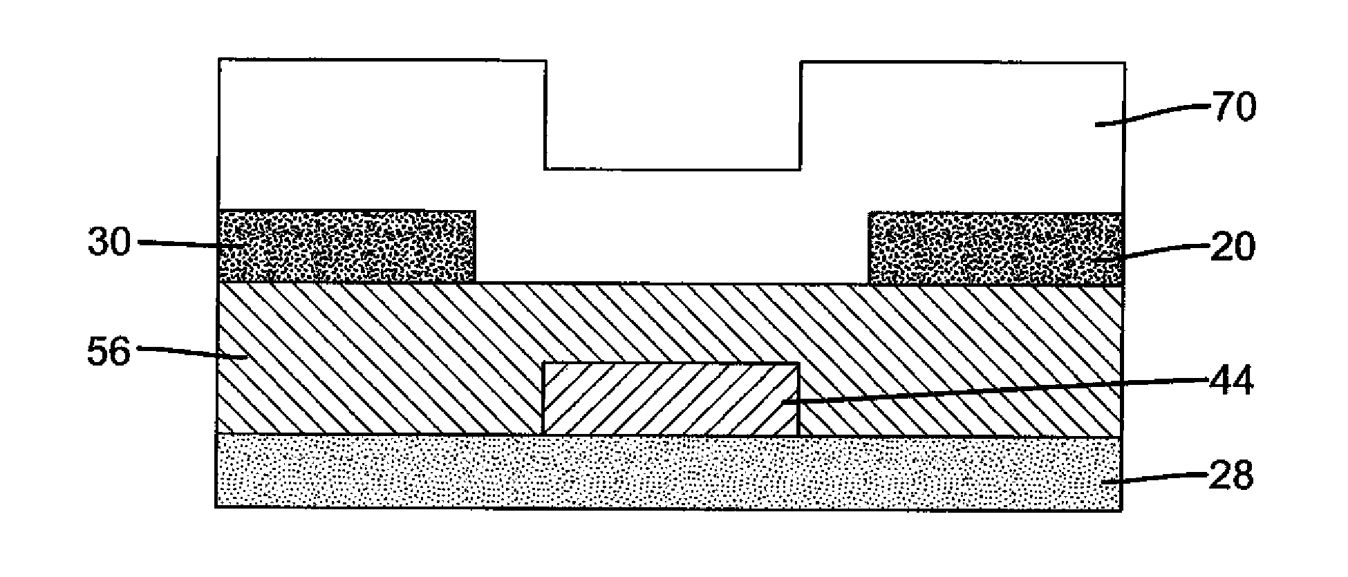
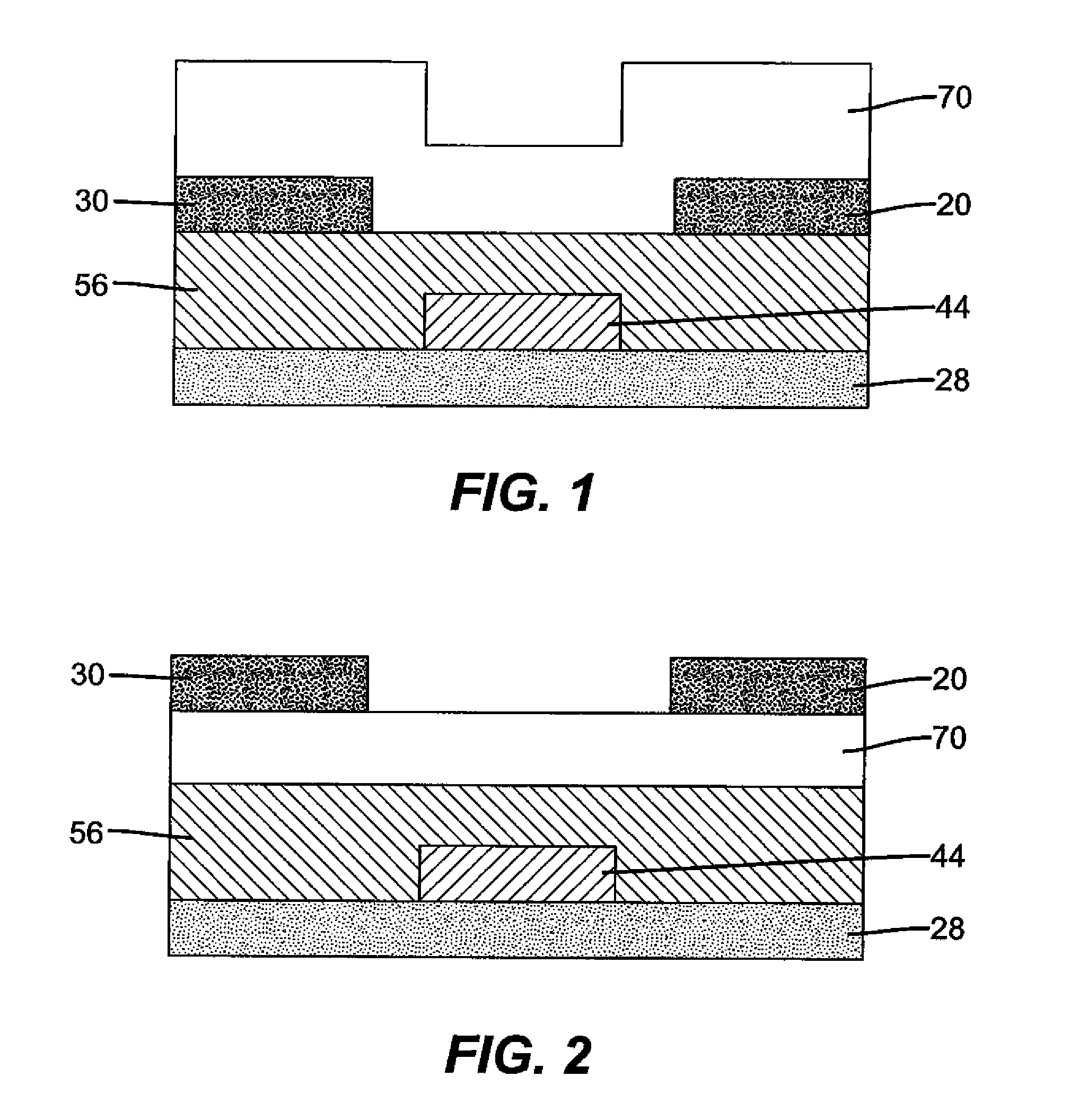
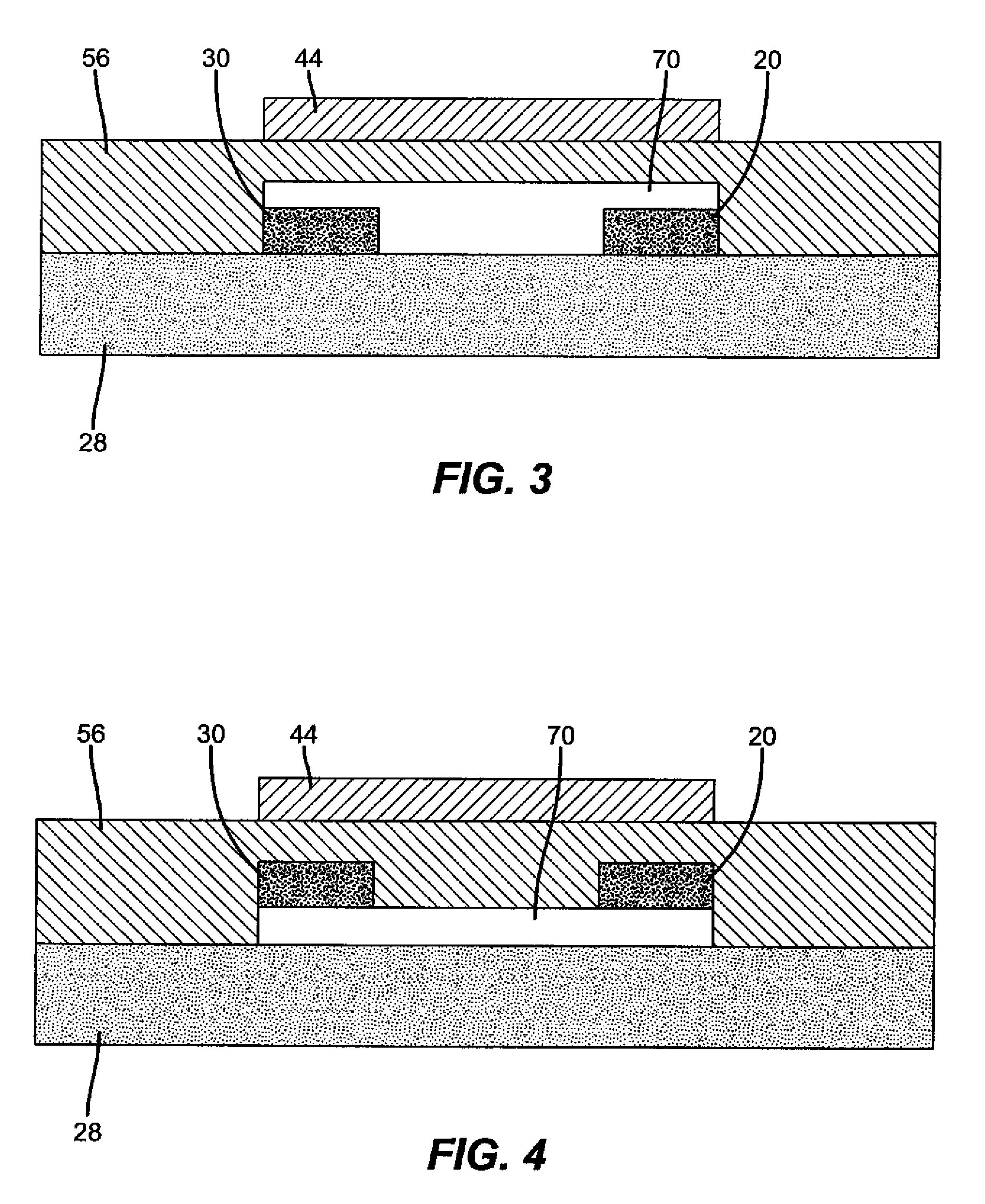
FIELD OF THE INVENTION[0001]The present invention relates to the use of zinc-oxide-based semiconductor materials in semiconductor films for thin film transistors. Such thin film transistors can be used in electronic devices, particularly in displays in which solution processable semiconductor materials, and low temperature processes of making the same, are advantageous.BACKGROUND OF THE INVENTION[0002]Thin film transistors (TFTs) are widely used as switching elements in electronics, for example, in active-matrix liquid-crystal displays, smart cards, and a variety of other electronic devices and components thereof. The thin film transistor (TFT) is an example of a field effect transistor (FET). The best-known example of an FET is the MOSFET (Metal-Oxide-Semiconductor-FET), today's conventional switching element for high-speed applications. For applications in which a transistor needs to be applied to a substrate, a thin film transistor is typically used. A critical step in fabricatin...

Claims


Application Information

Patent Timeline
Patent Type & Authority Patents(United States)
IPC IPC(8): H01L21/20
CPCB82Y10/00H01L21/02554H01L29/7869H01L21/02601H01L21/02628H01L21/02579Y10S977/811Y10S977/938
Inventor LEVY, DAVID H.SCUDERI, ANDREA C.IRVING, LYN M.
Owner EASTMAN KODAK CO
Why Eureka
Try Eureka