

Field effect transistor manufacturing method
- Summary
- Abstract
- Description
- Claims
- Application Information
AI Technical Summary
Benefits of technology
Problems solved by technology
Method used
Image

Examples
first embodiment
Pre-Deposition to Post-Deposition
1-A
[0074] The method for manufacturing a field effect transistor according to the present embodiment is characterized by, subsequent to preparing a substrate yet prior to forming on the substrate an active layer comprising an amorphous oxide, carrying out any of the following steps:
[0075] irradiating ultraviolet rays onto the substrate surface in an ozone atmosphere; or
[0076] irradiating plasma onto the substrate surface; or
[0077] cleaning the substrate surface with a chemical solution containing hydrogen peroxide; or
[0078] coating with a film comprising silicon and oxygen.
[0079] As a result of the above surface treatment process of the substrate, contaminants adhered to the substrate surface are removed, whereby the substrate surface is cleaned.
[0080] As a result of the above process, performance deterioration due to contaminants diffusing into the film constituting a TFT (thin-film transistor), or other such field effect transistor, can be...
example 1-1
[0341] First, a PET substrate is placed in the chamber of a UV / O3 surface treatment apparatus, and the substrate surface is irradiated with ultraviolet rays.
[0342] The chamber that this apparatus has conducts deposition in an oxygen-containing atmosphere under atmospheric pressure. Ozone forms in the chamber from the ultraviolet ray irradiation. Contaminants on the substrate surface are removed by the ozone and the ultraviolet rays, whereby a clean surface can be obtained.
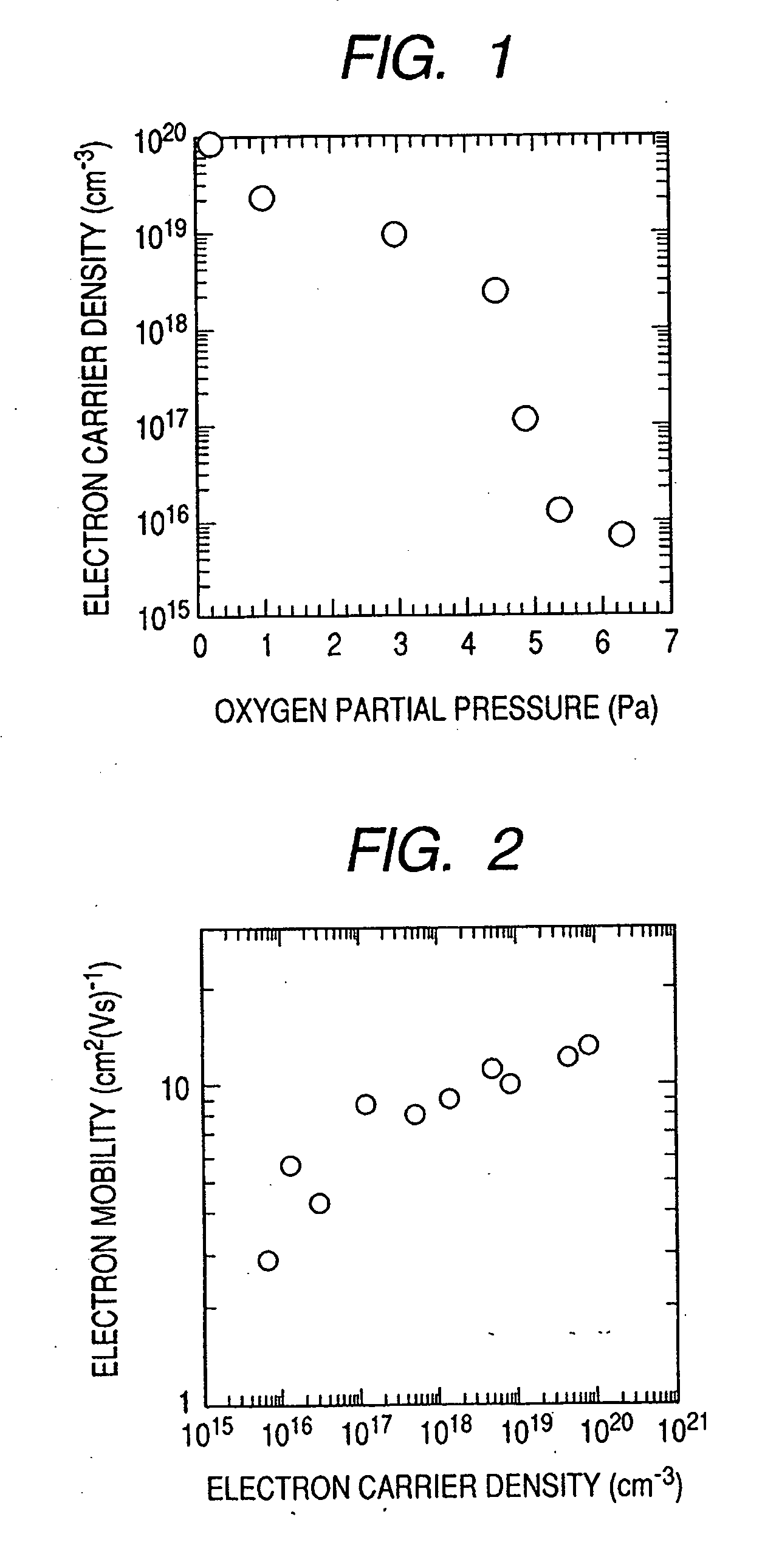
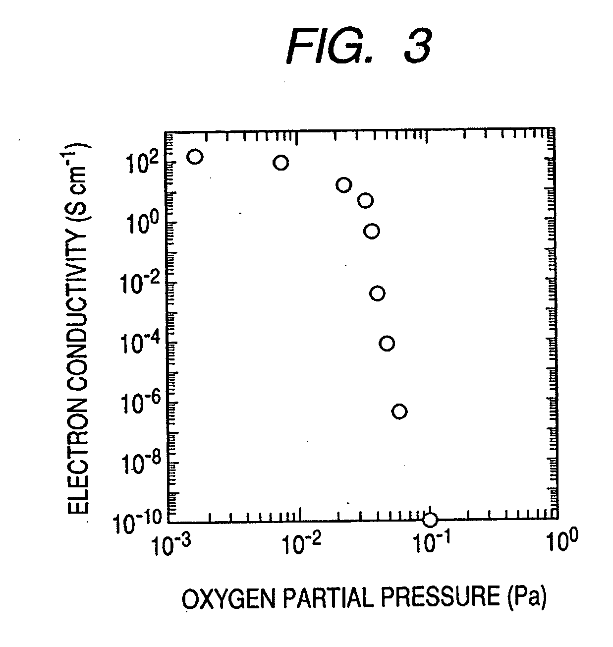
[0343] On a substrate which had undergone surface treatment using this method, an In—Ga—Zn—O system amorphous oxide semiconductor thin-film is deposited by pulsed laser deposition employing a KrF excimer laser with a polycrystalline sintered body having an InGaO3(ZnO)4 composition serving as the target.
[0344] The deposition conditions are appropriately set within the above-mentioned range.
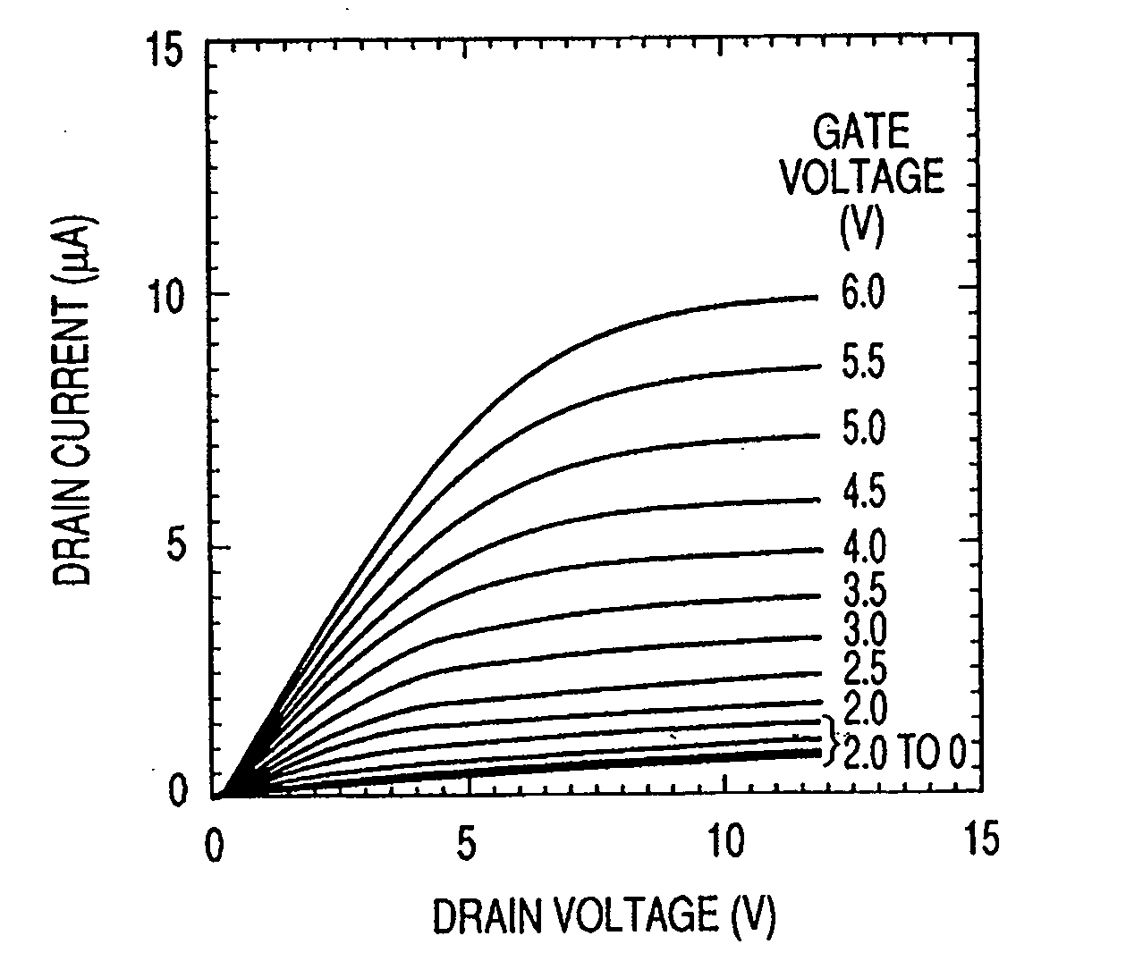
[0345] Next, the top-gate type MISFET device illustrated in FIG. 5 will be fabricated. Specifically, the device is fabricate...
example 1-2
[0348] First, a glass substrate (1737, manufactured by Corning Incorporated) is placed in the chamber of a parallel-plate atmospheric-pressure plasma apparatus, and low-energy plasma is irradiated onto the substrate surface.
[0349] This apparatus removes contaminants on the substrate surface by irradiating low-energy plasma onto the substrate surface, whereby the state of the substrate top surface can be made to change.
[0350] On a substrate which had undergone surface treatment using this method, an In—Ga—Zn—O system amorphous oxide semiconductor thin-film is deposited by pulsed laser deposition employing a KrF excimer laser with a polycrystalline sintered body having an InGaO3(ZnO)4 composition serving as the target.
[0351] It can be confirmed from a peeling test carried out on the obtained amorphous oxide film that the adhesion between the substrate and the amorphous oxide film is extremely good.
[0352] An amorphous oxide obtained in this manner can be used to fabricate a transis...
PUM
 Abstract
Description
Claims
Application Information