Thin film transistor having a two-layer semiconductor, manufacturing method therefor, and display apparatus using the same

a technology of thin film transistor and manufacturing method, which is applied in the direction of transistors, semiconductor devices, electrical devices, etc., can solve the problems of uniform display image and inhibit unstable operation

Inactive Publication Date: 2012-05-31
CANON KK
View PDF4 Cites 111 Cited by
  • Summary
  • Abstract
  • Description
  • Claims
  • Application Information

AI Technical Summary

Benefits of technology

[0014]On the other hand, it is known that the oxide semiconductor decreases its electric resistance when oxygen is deficient therein, because of generating a carrier.
[0016]Accordingly, an object of the present invention is to improve the dispersion of the characteristics among the TFTs due to the ununiformity of the damage which the semiconductor layer receives when the protective layer is formed with the sputtering technique, and to enhance the uniformity of the image in the active matrix type display apparatus which employs the improved TFT.
[0020]A manufacturing method according to the present invention includes oxidizing the back channel layer of the semiconductor layer up to a deeper position than the damaged layer formed therein when the protective layer is formed. Thereby, the method oxidizes the damaged layer to passivate the damaged layer, and can effectively inhibit an adverse effect exerted on electrical conduction characteristics in the channel region of the thin film transistor. That is, the present invention can improve the dispersion of characteristics among the TFTs due to the ununiformity of damage which the semiconductor layer receives when the protective layer is formed with the sputtering method and enhance the uniformity of the image in the active matrix type display apparatus using the improved TFT.
[0021]As a result, the method can inhibit the dispersion of the characteristics among a plurality of the TFTs.
[0022]In addition, the present invention can provide an active matrix type display apparatus which shows a uniform image by using a pixel drive circuit constituted by TFTs according to the present invention.

Problems solved by technology

Such a technology can inhibit the unstable operation due to the change of the ambient atmosphere to some extent.
However, it has been found that a bottom gate type TFT occasionally produces the dispersion of the characteristics among a plurality of TFTs manufactured at the same time, which has not been observed at a stage before the protective layer is formed.
In addition, when an active matrix type of a display apparatus employs the TFT which produces such a dispersion of the characteristics, the apparatus has caused the ununiformity of the displayed image.

Method used


Image

  • Thin film transistor having a two-layer semiconductor, manufacturing method therefor, and display apparatus using the same
  • Thin film transistor having a two-layer semiconductor, manufacturing method therefor, and display apparatus using the same
  • Thin film transistor having a two-layer semiconductor, manufacturing method therefor, and display apparatus using the same

Examples


example 1

[0101]In the present Example, a TFT including a columnar structure in a semiconductor layer will now be described below.

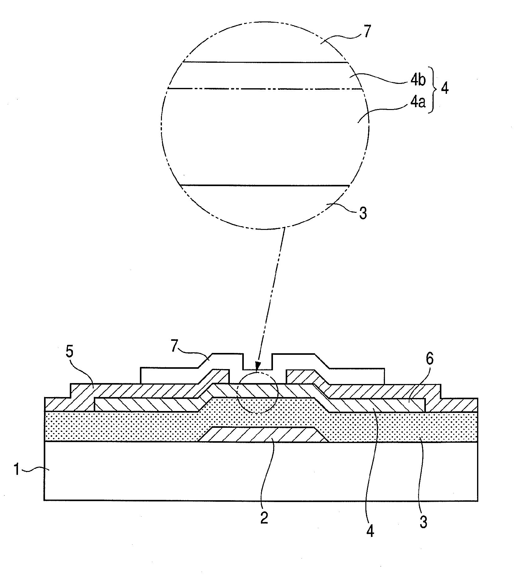
[0102]A bottom gate type TFT provided with a protective layer as illustrated in FIG. 2 is prepared with the use of a glass substrate.

[0103]At first, a metallic multilayer film including Ti of 5 nm, Mo of 40 nm and Ti of 5 nm is formed on the glass substrate with a sputtering technique which uses a Ti target and an Mo target. This metal film is patterned with a photolithographic technique to be formed into a gate electrode.

[0104]A film of amorphous SiOx of 200 nm is formed thereon with the sputtering technique which uses SiO2 as the target, and is formed into a gate insulation layer. At this time, Ar is used as a sputtering gas.

[0105]An amorphous oxide semiconductor film of 40 nm including In—Zn—Ga—O is formed thereon with the sputtering technique which uses In—Zn—Ga—O as the target. A semiconductor layer is then formed by patterning the semiconductor film with the ...

example 2

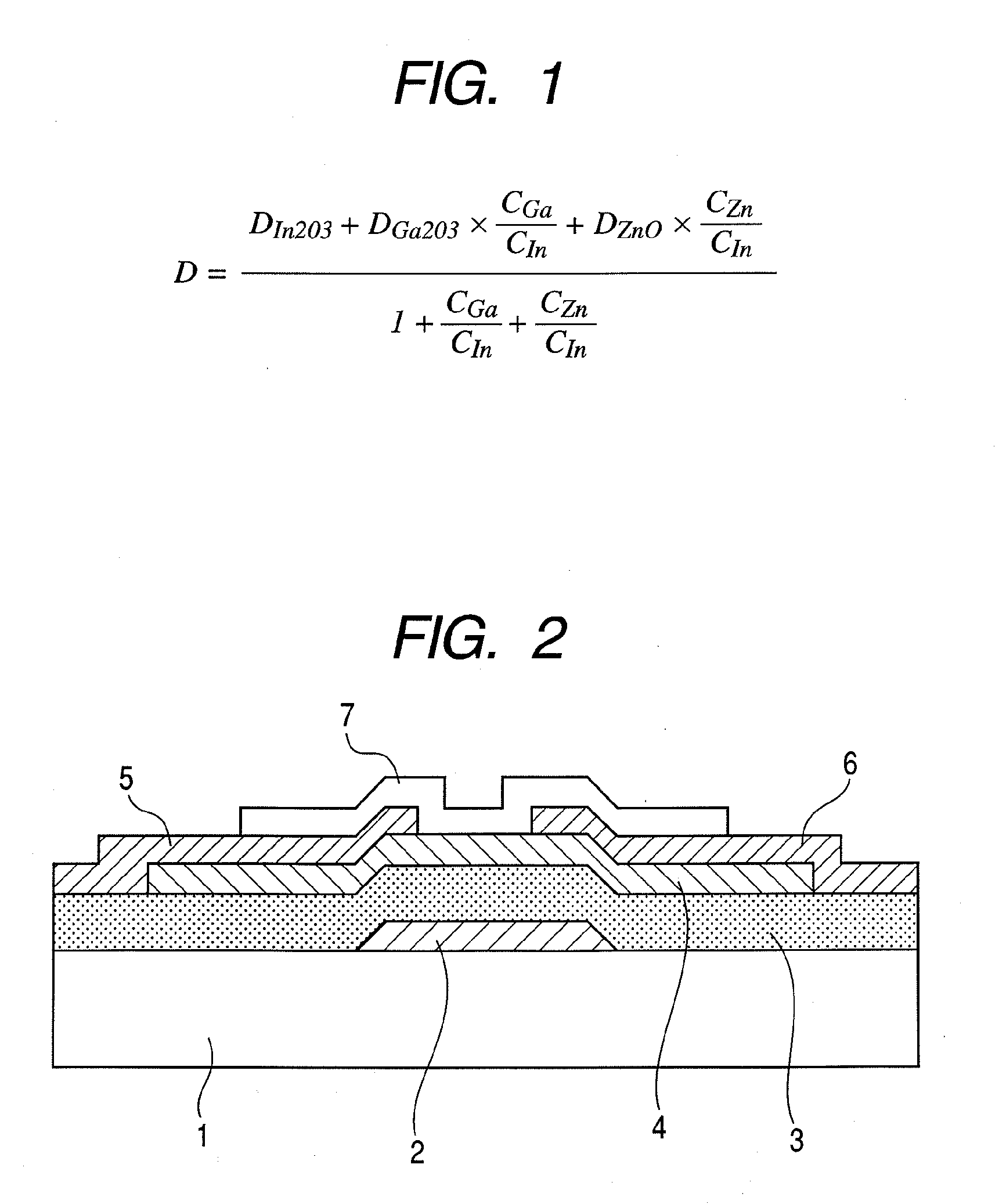
[0115]In the present Example, a TFT including a semiconductor layer made of a first layer having high mass density and a second layer having low mass density will now be described below.

[0116]A bottom gate type TFT provided with a protective layer as illustrated in FIG. 9 is prepared with the use of an n-type Si substrate.

[0117]At first, a thermal oxidation Si film (gate insulation film 93) is formed in a thickness of 100 nm on an n-type Si substrate 92. In FIG. 9, an independent gate electrode is not provided, but the n-type Si substrate 92 functions as a gate electrode. An amorphous oxide semiconductor film (first layer) including In—Zn—Ga—O is formed thereon into 30 nm with a sputtering technique which employs In—Zn—Ga—O as a target and room temperature as a substrate temperature. Furthermore, an amorphous oxide semiconductor film (second layer) including In—Zn—Ga—O is formed thereon into 10 nm with a PLD technique which employs room temperature as a substrate temperature. The tw...

example 3

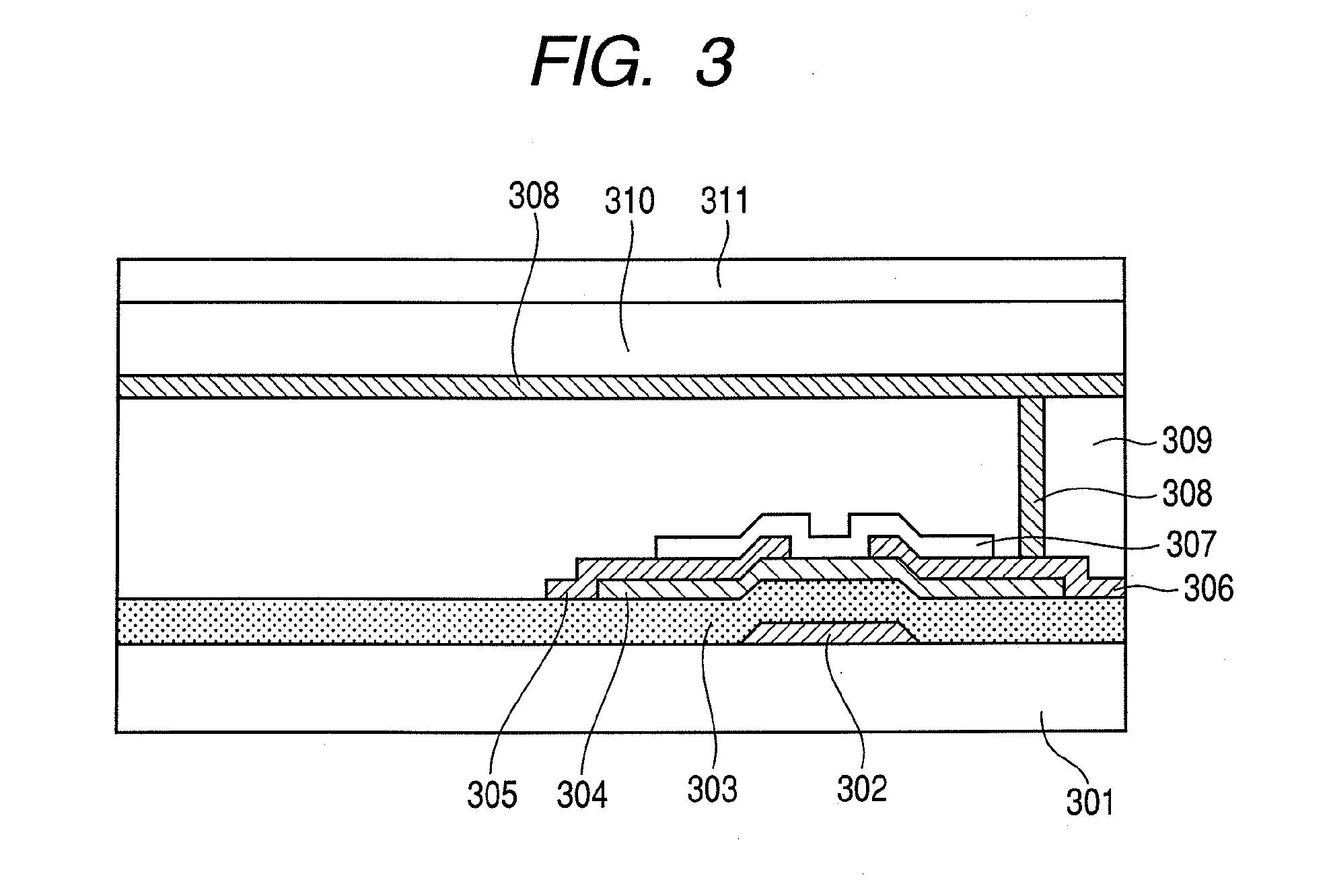
[0127]In the present Example, a display apparatus using a TFT in FIG. 3 will now be described.

[0128]A TFT is manufactured in a process similar to that in Example 1.

[0129]After the TFT has been prepared, an interlayer insulation film 309 is formed. At this time, a contact hole for connecting a drain electrode 305 with a lower electrode 308 is formed.

[0130]Subsequently, a lower electrode 308 is formed thereon by forming a film of Al with an electron beam vapor deposition technique. The lower electrode 308 is connected with the drain electrode 305 through the contact hole.

[0131]Next, an electron transport layer, a light-emitting layer, a hole transport layer, a hole injection layer are sequentially formed with a vapor deposition technique, which form an organic EL light-emitting layer as a whole.

[0132]Finally, an upper electrode 311 is formed thereon by forming a film of ITO with a sputtering technique.

[0133]Here, when voltage is applied to a source electrode 306 of the TFT and voltage...


PUM


Abstract

A transistor is constituted of a gate electrode 2, a gate insulation layer 3, a semiconductor layer 4 formed of an amorphous oxide, a source electrode 5, a drain electrode 6 and a protective layer 7. The protective layer 7 is provided on the semiconductor layer 4 in contact with the semiconductor layer 4, and the semiconductor layer 4 includes a first layer at least functioning as a channel layer and a second layer having higher resistance than the first layer. The first layer is provided on the gate electrode 2 side of the semiconductor layer 4 and the second layer is provided on the protective layer 7 side of the semiconductor layer 4.

Description

RELATED APPLICATIONS[0001]This application is a divisional of application Ser. No. 12 / 672,103, filed Feb. 4, 2010. It claims benefit of that application under 35 U.S.C. §120, and claims benefit under 35 U.S.C. §119 of Japanese Patent Applications Nos. 2007-254364 and 2008-196038, filed on Sep. 28, 2007, and Jul. 30, 2008, respectively. The entire contents of each of the mentioned prior applications are incorporated herein by reference.TECHNICAL FIELD[0002]The present invention relates to a thin film transistor, a manufacturing method therefor, and a display apparatus using the same, and particularly to a thin film transistor which has improved dispersion of characteristics among TFTs, a manufacturing method therefor, and a display apparatus using the same.BACKGROUND OF THE INVENTION[0003]1. Field of the Invention[0004]In recent years, developments have proceeded on a TFT which uses a transparent oxide semiconductor as an active layer.[0005]US2006 / 108636 A1 discloses a technology on ...

Claims


Application Information

Patent Timeline
Patent Type & Authority Applications(United States)
IPC IPC(8): H01L29/786
CPCH01L29/78606H01L29/7869H01L29/66969H01L33/0054H01L33/16H01L29/78696H01L21/324H01L29/66742H01L29/78693
Inventor SHIMADA, MIKIOHAYASHI, RYOKUMOMI, HIDEYA
Owner CANON KK
Why Eureka
Try Eureka