

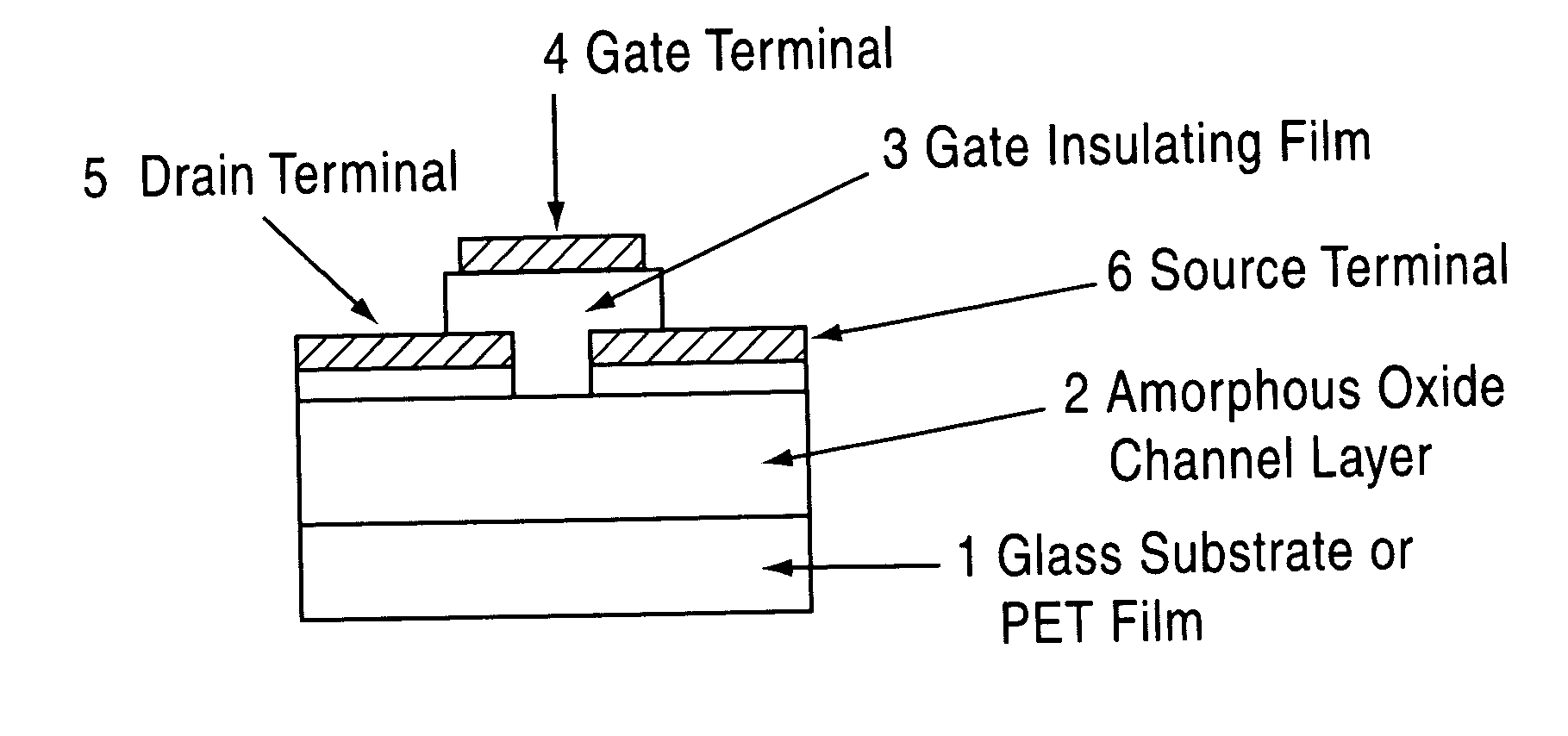
Amorphous Oxide And Thin Film Transistor
a thin film transistor and amorphous oxide technology, applied in non-linear optics, instruments, vacuum evaporation coatings, etc., can solve the problems of difficult to decrease the electrical conductivity, difficult to increase the on/off ratio of the transistor, and the inability to increase the electron mobility
- Summary
- Abstract
- Description
- Claims
- Application Information
AI Technical Summary
Benefits of technology
Problems solved by technology
Method used
Image

Examples
example 1
Preparation of Amorphous In—Ga—Zn—O Thin Film by PLD Method
[0053] A film was formed in a PLD device shown in FIG. 7. In the drawing, reference numeral 701 denotes a rotary pump (RP), 702 denotes a turbo molecular pump (TMP), 703 denotes a preparation chamber, 704 denotes en electron gun for RHEED, 705 denotes a substrate holder for rotating and vertically moving the substrate, 706 denotes a laser entrance window, 707 denotes a substrate, 708 denotes a target, 709 denotes a radical source, 710 denotes a gas inlet, 711 denotes a target holder for rotating and vertically moving the target, 712 denotes a by-pass line, 713 denotes a main line, 714 denotes a turbo molecular pump (TMP), 715 denotes a rotary pump (RP), 716 denotes a titanium getter pump, and 717 denotes a shutter. In the drawing, 718 denotes ionization gauge (IG), 719 denotes a Pirani gauge (PG), 720 denotes a Baratron gauge (BG), and 721 denotes a deposition chamber.
[0054] An In—Ga—Zn—C amorphous oxide semiconductor thin...
example 2
Formation of Amorphous InGaO3(ZnO) and InGaO3(ZnO)4 Oxide Films by PLD Method
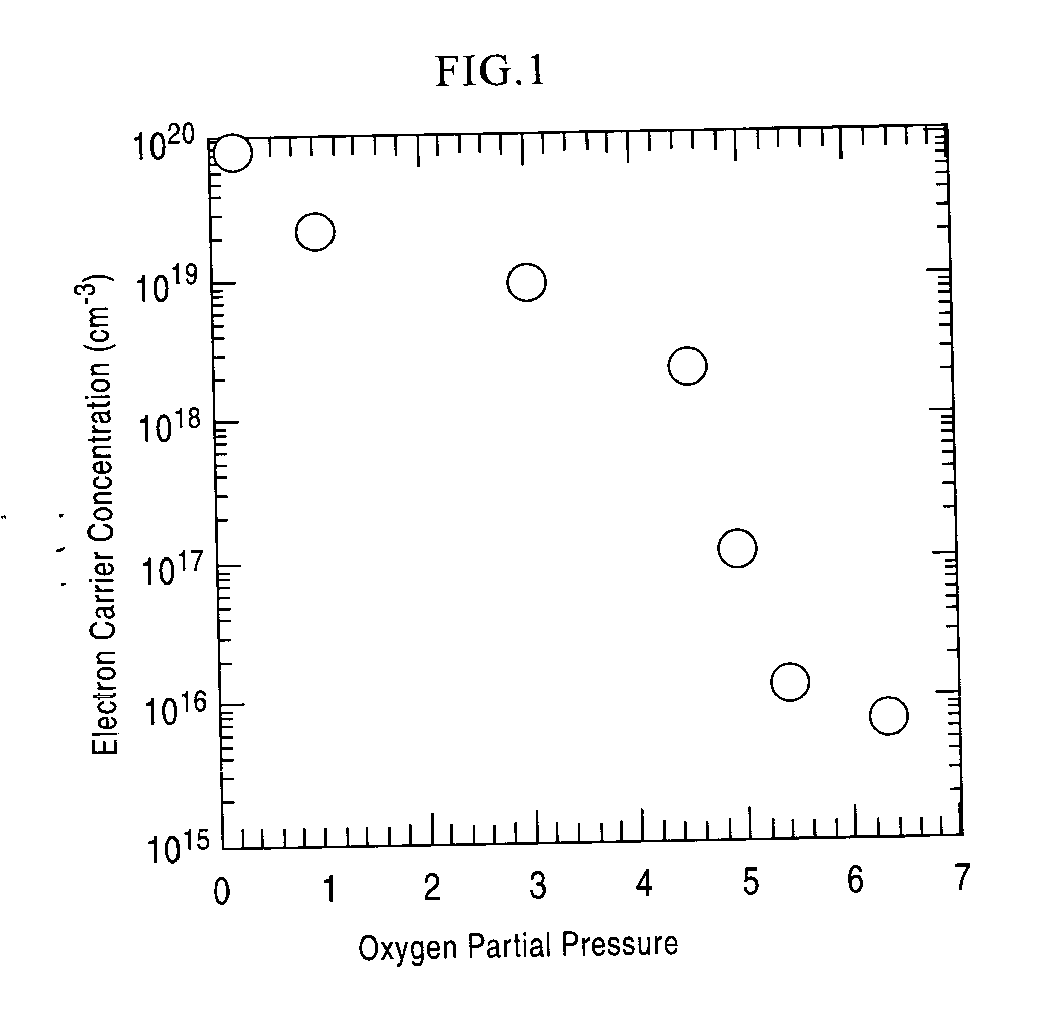
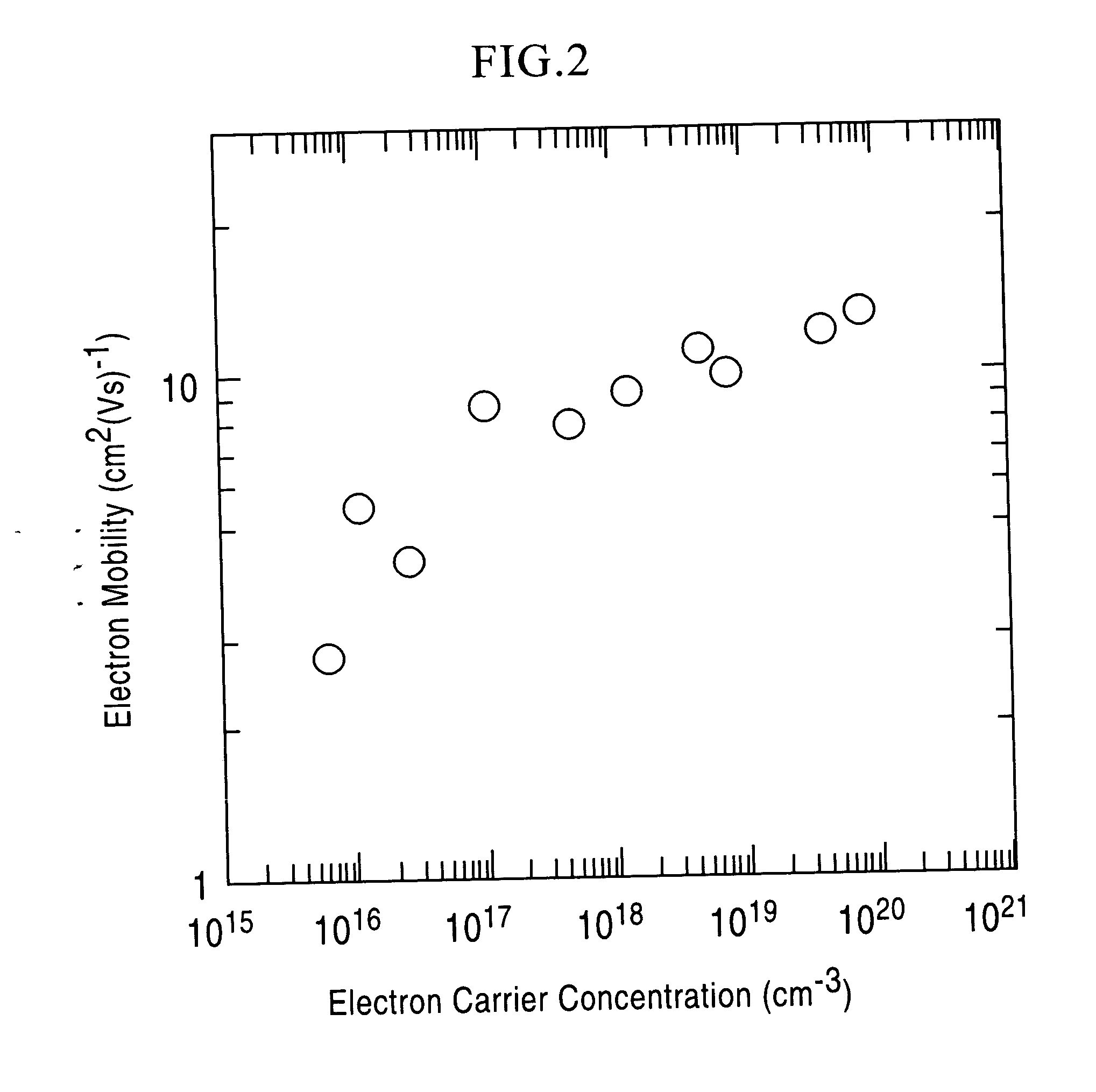
[0070] In—Zn—Ga—O amorphous oxide films were deposited on glass substrates (#1737 produced by Corning) by using polycrystalline sinters represented by InGaO3(ZnO) and InGaO3(ZnO)4 as the targets by a PLD method using KrF excimer laser. The same PLD deposition device as shown in EXAMPLE 1 was used, and the deposition was conducted under the same conditions. The substrate temperature during the deposition was 25° C.
[0071] Each film obtained thereby was subjected to grazing incidence x-ray diffraction (thin film method, incident angle: 0.5°) for the film surface. No clear diffraction peak was detected. The In—Zn—Ga—O films prepared from the two targets were both amorphous.
[0072] The In—Zn—Ga—O amorphous oxide films on the glass substrates were each analyzed to determine the x-ray reflectance. Analysis of the pattern found that the root mean average roughness (Rrms) of the thin film was about 0.5 mm and that...
example 3
Formation of In—Zn—Ga—O Amorphous Oxide Film by SP Method
[0078] Formation of a film by a high-frequency SP method using argon gas as the atmosphere gas is described. The SP method was conducted using the device shown in FIG. 8. In the drawing, reference numeral 807 denotes a substrate for deposition, 808 denotes a target, 805 denotes a substrate holder equipped with a cooling mechanism, 814 denotes a turbo molecular pump, 815 denotes a rotary pump, 817 denotes a shutter, 818 denotes an ionization gauge, 819 denotes a Pirani gauge, 821 denotes a deposition chamber, and 830 denotes a gate valve. A SiO2 glass substrate (#1737 produced by Corning) was used as the substrate 807 for deposition. As the pre-deposition treatment, the substrate was degreased with ultrasonic waves in acetone, ethanol, and ultrapure water for 5 minutes each, and then dried in air at 100° C.
[0079] An InGaO3(ZnO)4 polycrystalline sinter (size: 20 mm in dia., 5 mm in thickness) was used as the target material. T...
PUM
| Property | Measurement | Unit |
|---|---|---|
| electron mobility | aaaaa | aaaaa |
| electron mobility | aaaaa | aaaaa |
| temperature | aaaaa | aaaaa |
Abstract
Description
Claims
Application Information