

Field-effect transistor including transparent oxide and light-shielding member, and display utilizing the transistor
a field-effect transistor and light-shielding member technology, applied in the direction of instruments, semiconductor devices, electrical apparatus, etc., can solve the problems affecting the stable performance of the
- Summary
- Abstract
- Description
- Claims
- Application Information
AI Technical Summary
Benefits of technology
Problems solved by technology
Method used
Image


Examples
first embodiment
Incident Light from Substrate Side
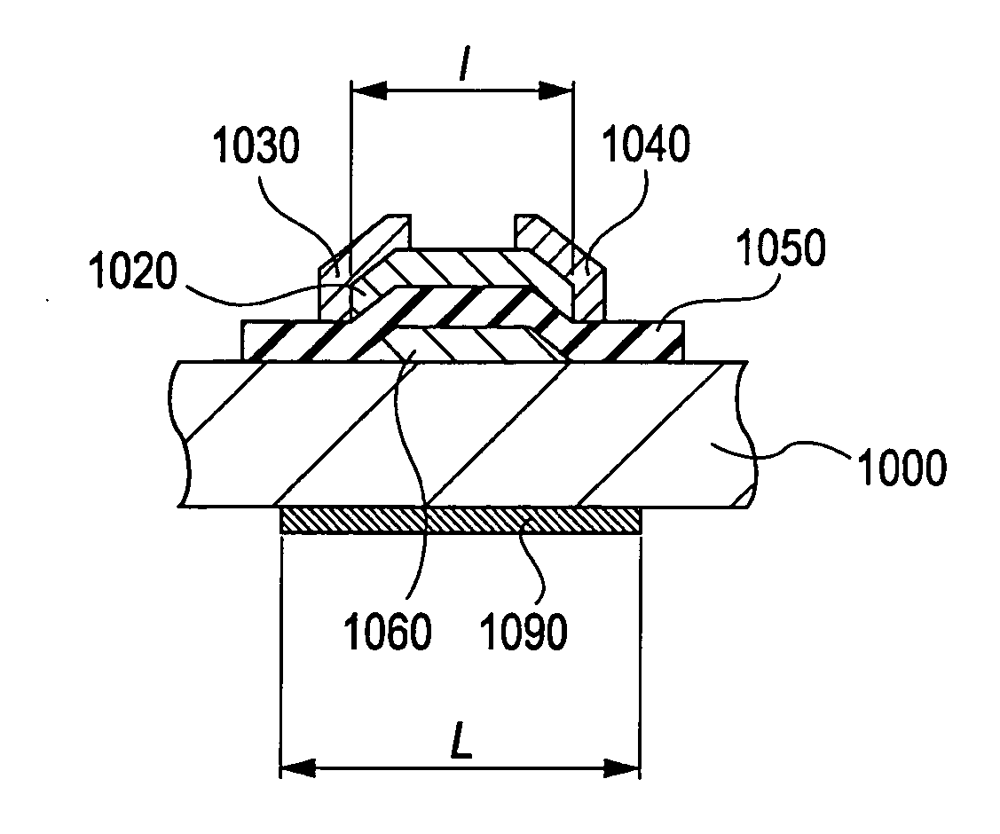
[0031] Light entering from the substrate side toward the active layer is shielded when light-shielding films are provided at the positions shown in FIGS. 1 to 3.
[0032] Preferably, the light-shielding film has a light-shielding property to visible light having a wavelength range of 400 to 800 nm. More preferably, the light-shielding film further has a light-shielding property to light or an electromagnetic wave having a wavelength of 400 nm or less (for example, the wavelength range of 100 to 400 nm).
[0033] The transparent oxide (for example, transparent amorphous oxide) in the present invention causes a phenomenon of photocarrier generation in the shorter-wavelength region of visible light. Therefore, in particular, it is preferable that the light-shielding film have a light-shielding property to at least light or an electromagnetic wave having a wavelength range of 300 to 500 nm.
[0034] In addition, the light-shielding film is not required to hav...
second embodiment
ncident Light from the Side Opposite the Substrate
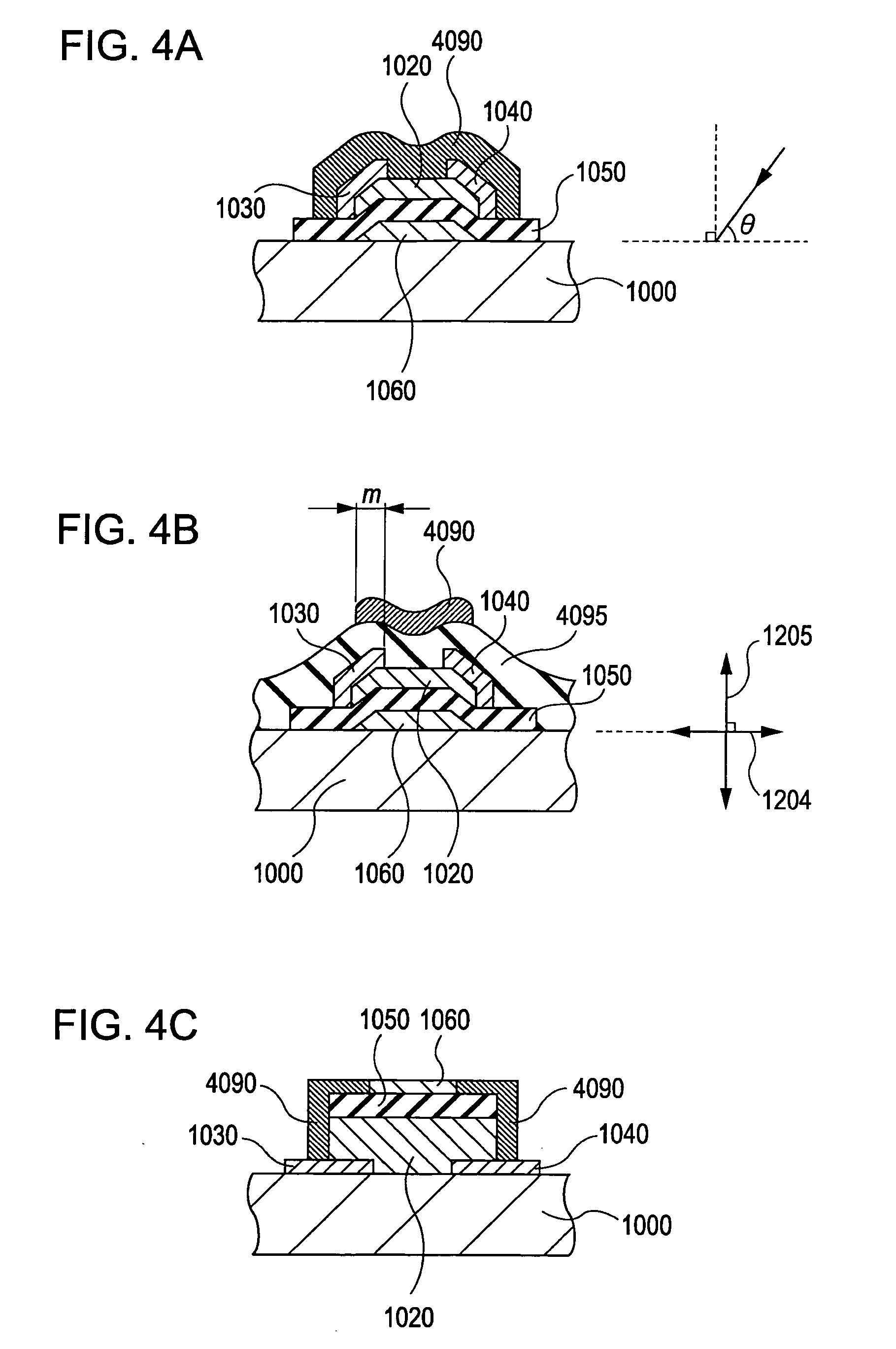
[0043] In order to shield the incident light from the side opposite the substrate, a light-shielding film 4090 is provided as shown in FIG. 4A.
[0044] Preferably, the light-shielding film 4090 has a light-shielding property to visible light having a wavelength range of 400 to 800 nm. More preferably, the light-shielding film further has a light-shielding property to an electromagnetic wave having a wavelength of 400 nm or less (for example, the wavelength range of 100 to 400 nm).
[0045] The transparent oxide (for example, amorphous oxide) in the present invention causes a phenomenon of photocarrier generation in the shorter-wavelength region of visible light. Therefore, in particular, it is preferable that the light-shielding film have a light-shielding property to at least light or an electromagnetic wave having a wavelength range of 300 to 500 nm.
[0046] In addition, the light-shielding film is not required to have a transmittance ...
third embodiment
[0053] A display provided with a field-effect transistor (specifically TFT) described in the first or second embodiment will now be described.
[0054] The structure used in a display is as follows:
[0055] The drain electrode functioning as an output terminal of a TFT is connected to an input electrode of a light-emitting device such as an electroluminescence device using an organic or inorganic material, a light-transmittance-controlling device of a liquid-crystal cell or an electrophoretic particle cell, or a light-reflectance-controlling device.
[0056] For example, as shown in FIG. 5, an amorphous oxide semiconductor film 5002, a source electrode 5003, a drain electrode 5004, a gate-insulating film 5005, and a gate electrode 5006 are deposited and patterned on a substrate 5001.
[0057] The drain electrode 5004 is connected to an electrode 5008 via an interlayer-insulating film 5007. The electrode 5008 is in contact with a light-emitting layer 5010 which is in contact with an electro...
PUM
 Abstract
Description
Claims
Application Information