METHOD OF FABRICATING ZnO FILM AND THIN FILM TRANSISTOR ADOPTING THE ZnO FILM

a thin film transistor and zno film technology, applied in the direction of coatings, semiconductor devices, chemical vapor deposition coatings, etc., can solve the problems of inability to use plastic substrates, heavy and inflexible tft-lcds, and inability to fabricated flexible displays

Inactive Publication Date: 2007-07-26
SAMSUNG ELECTRONICS CO LTD +1
View PDF7 Cites 4045 Cited by
  • Summary
  • Abstract
  • Description
  • Claims
  • Application Information

AI Technical Summary

Problems solved by technology

TFT-liquid crystal displays (“LCDs”) using silicon use glass substrates and thus are heavy and inflexible.
Thus, the TFT-LCDs may not be fabricated as flexible displays.
However, such high temperature film growth is used in limited substrate materials and thus cannot be used for plastic substrates or the like, which have a low heat resistance.
However, it is difficult to adjust component ratios of In, Ga, and Zn, and the oxide cannot be grown using a MOCVD method.
As a result, it is difficult to mass-produce ZnO films.

Method used


Image

  • METHOD OF FABRICATING ZnO FILM AND THIN FILM TRANSISTOR ADOPTING THE ZnO FILM
  • METHOD OF FABRICATING ZnO FILM AND THIN FILM TRANSISTOR ADOPTING THE ZnO FILM
  • METHOD OF FABRICATING ZnO FILM AND THIN FILM TRANSISTOR ADOPTING THE ZnO FILM

Examples


Embodiment Construction

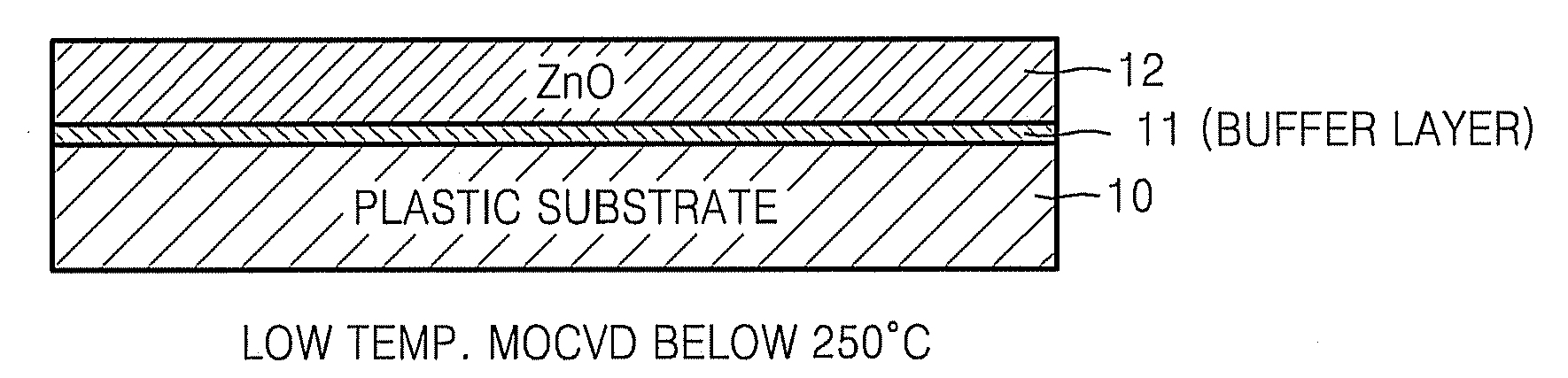
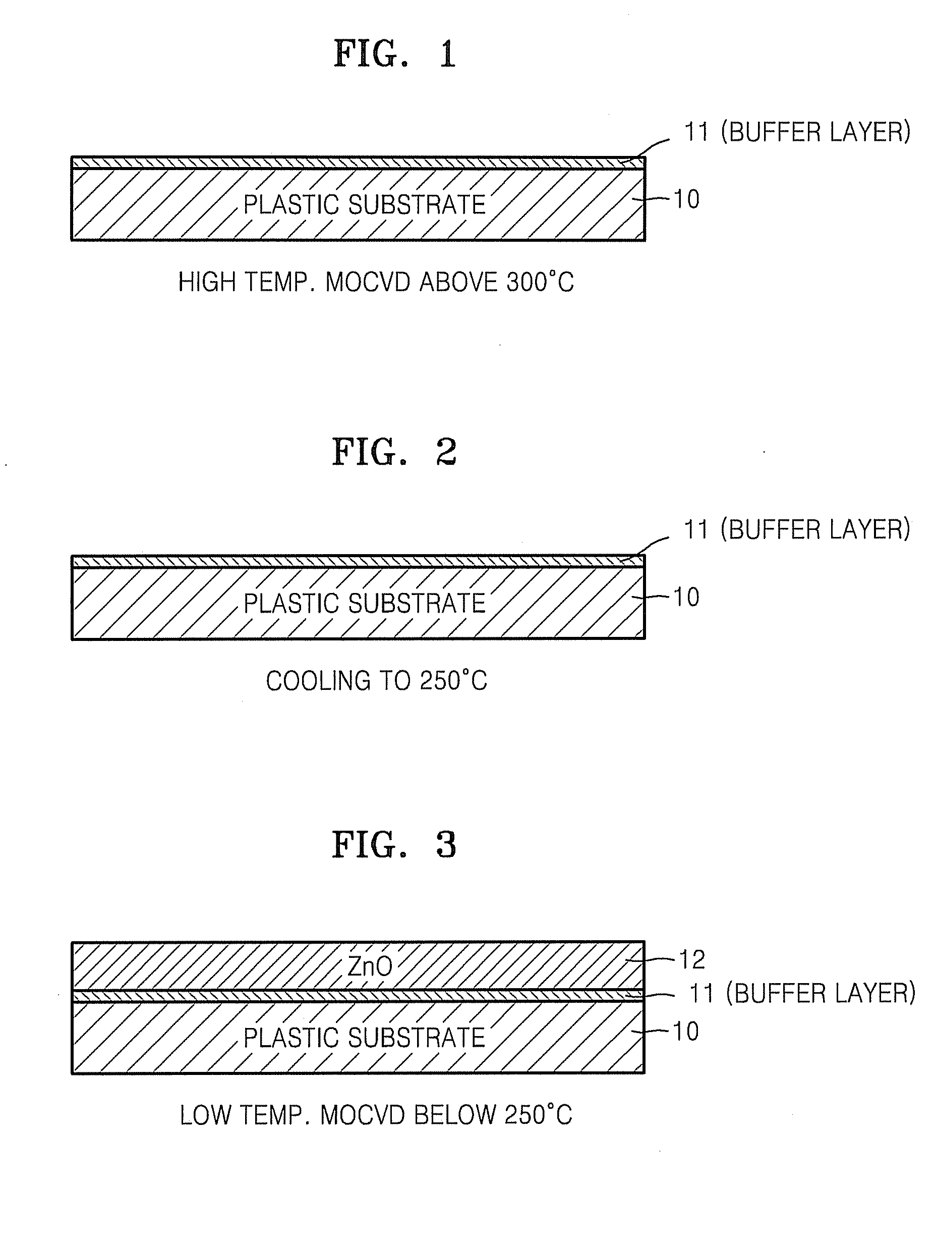
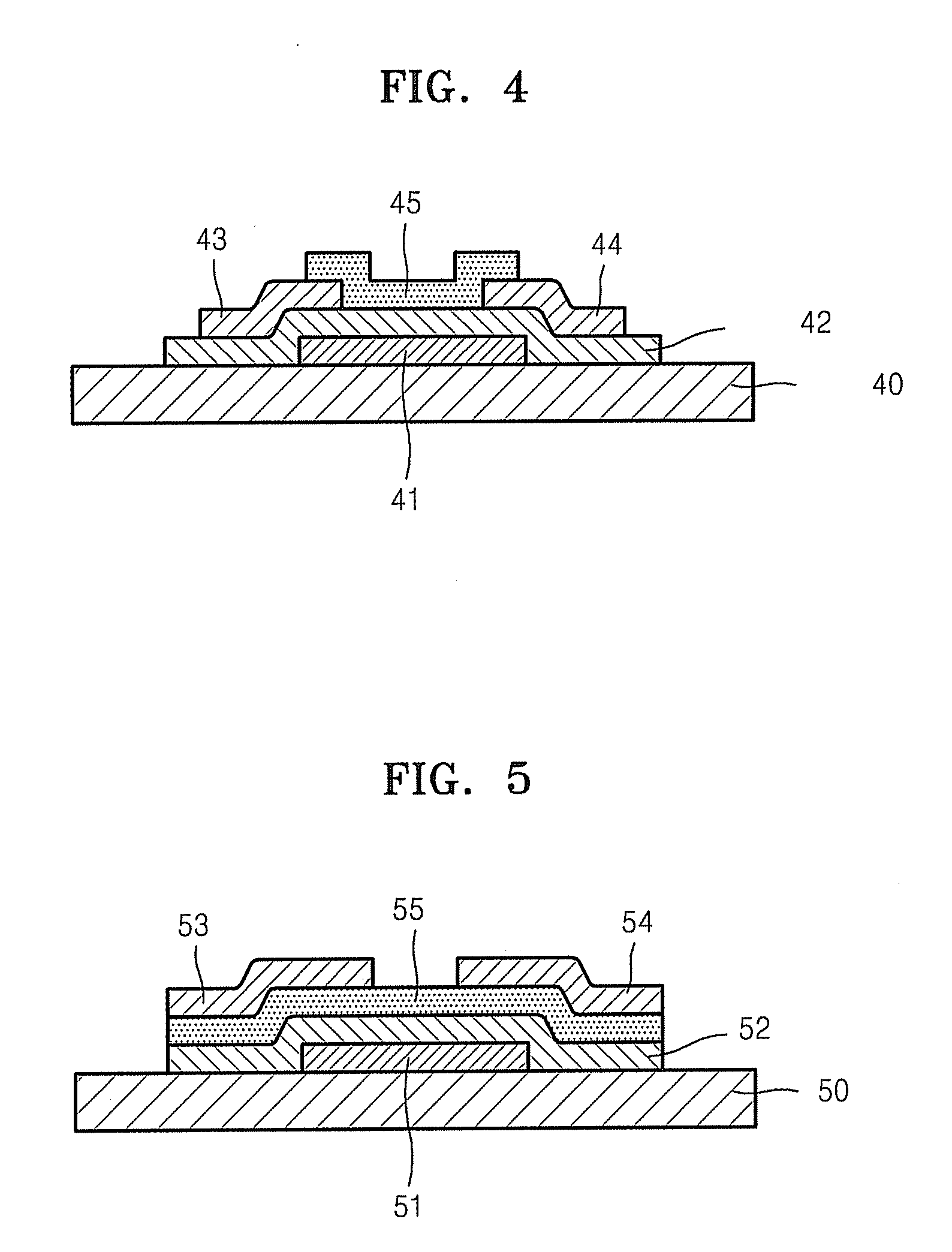
[0017]Hereinafter, a method of fabricating a ZnO semiconductor film and a ZnO thin film transistor (TFT) will be described.

[0018]It will be understood that when an element is referred to as being “on” another element, it can be directly on the other element or intervening elements may be present therebetween. In contrast, when an element is referred to as being “disposed on” another element, the elements are understood to be in at least partial contact with each other, unless otherwise specified.

[0019]The terminology used herein is for the purpose of describing particular embodiments only and is not intended to be limiting of the invention. As used herein, the singular forms “a”, “an” and “the” are intended to include the plural forms as well, unless the context clearly indicates otherwise. It will be further understood that the terms “comprises” and / or “comprising,” or “includes” and / or “including” when used in this specification, specify the presence of stated features, regions, i...


PUM

PropertyMeasurementUnit
temperatureaaaaaaaaaa
thicknessaaaaaaaaaa

Abstract

Provided is a method of fabricating a low temperature ZnO polycrystalline film and a thin film transistor (TFT) adopting the low temperature ZnO polycrystalline film. The method includes growing ZnO on a substrate at a first temperature for a first time using Metal Organic Chemical Vapor Deposition (MOCVD) to form a ZnO buffer layer, and heating the substrate at a temperature lower than the first temperature to grow ZnO on the ZnO buffer layer for a second time longer than the first time so as to form a ZnO film.

Description

CROSS-REFERENCE TO RELATED APPLICATION[0001]This application claims priority to Korean Patent Application No. 10-2006-0006569, filed on Jan. 21, 2006, and Korean Patent Application No. 10-2006-0125694, filed on Dec. 11, 2006, and all the benefits accruing therefrom under 35 U.S.C. § 119, the contents of which in their entirety are herein incorporated by reference.BACKGROUND OF THE INVENTION[0002]1. Field of the Invention[0003]The present invention relates to a method of fabricating a ZnO film, and more particularly, to a method of fabricating a ZnO film and a thin film transistor (“TFT”) adopting the ZnO film using low temperature Metal Organic Chemical Vapor Deposition (“MOCVD”).[0004]2. Description of the Related Art[0005]TFT-liquid crystal displays (“LCDs”) using silicon use glass substrates and thus are heavy and inflexible. Thus, the TFT-LCDs may not be fabricated as flexible displays. Organic semiconductor and metal oxide semiconductor materials have been recently studied to s...

Claims


Application Information

Patent Timeline
Patent Type & Authority Applications(United States)
IPC IPC(8): C23C16/00B05D7/00
CPCC23C16/0272C23C16/407H01L29/66969H01L29/7869H01L29/78603
Inventor SEO, O-GWEONJO, JUNGYOL
Owner SAMSUNG ELECTRONICS CO LTD
Why Eureka
Try Eureka