Semiconductor apparatus and method of manufacturing the same

a technology of amorphous oxide and a semiconductor, which is applied in the direction of semiconductor devices, electrical devices, basic electric elements, etc., can solve the problems of difficult formation of amorphous silicon tft and polysilicon, low thermal stability of polysilicon tft,

Inactive Publication Date: 2008-03-27
CANON KK
View PDF10 Cites 4075 Cited by
  • Summary
  • Abstract
  • Description
  • Claims
  • Application Information

AI Technical Summary

Benefits of technology

[0036]In order to solve the above-mentioned problems, according to the present invention, there is provided a semiconductor apparatus, including a plurality of kinds of field effect transistors, wherein the plurality of kinds of field effect transistors each include a channel layer made of an amorphous oxide containing a plurality of kinds of metal elements, and an element ratio of the amorphous oxide is changed so that the respective threshold voltages of the plurality of kinds of field effect transistors are different from one another.
[0037]Further, according to the present invention, there is provided a method of manufacturing a semiconductor apparatus, including forming a plurality of kinds of field effect transistors on a substrate and forming an oxide thin film as a channel layer formed of each of the field effect transistors, wherein in the formation of oxide thin film, at least two different materials are simultaneously supplied to the substrate from different directions.
[0038]Further, according to the present invention, there is provided a method of manufacturing a semiconductor apparatus, including forming a plurality of kinds of field effect transistors on a substrate and forming an oxide thin film as a channel layer of each of the field effect transistors, wherein material sources for supplying materials of the oxide thin film are disposed in rows, and in the formation of the oxide thin film, the substrate is moved in a direction different from a direction in which the material sources are disposed.

Problems solved by technology

However, it is difficult to form the amorphous silicon TFT and the polysilicon TFT on the substrate such as a plastic plate or a film because a high-temperature process is necessary for forming a device.
However, the organic semiconductor such as pentacene is disadvantageous in that thermal stability thereof is low (<150° C.
), so that a practical device is not realized.
However, a compound mainly made of ZnO cannot form a stable amorphous phase at room temperature, whereby it becomes a polycrystalline phase.

Method used


Image

  • Semiconductor apparatus and method of manufacturing the same
  • Semiconductor apparatus and method of manufacturing the same
  • Semiconductor apparatus and method of manufacturing the same

Examples


example 1

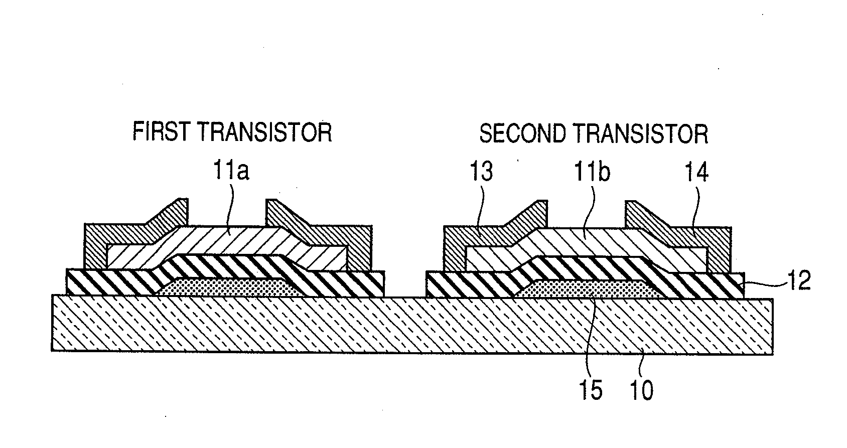
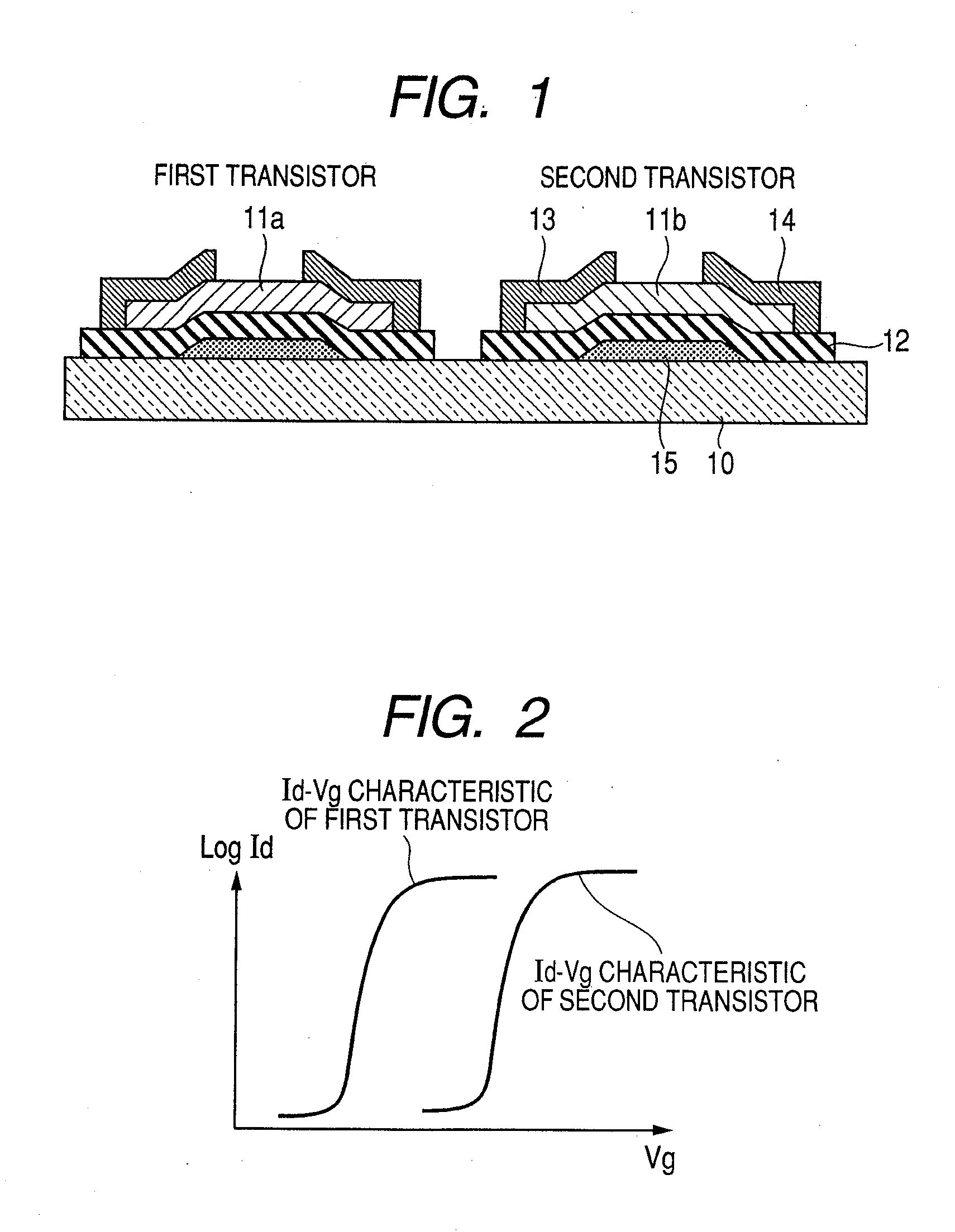
[0158]Example 1 is an example in which a semiconductor apparatus including bottom gate type TFT elements having different threshold voltages was formed on a glass substrate.

[0159]In Example 1, an In—Ga—Zn—O-based amorphous oxide is used for the channel layer 11a and 11b of the transistor. A channel length of the transistor is 60 μm, and a channel width thereof is 180 μm.

[0160]First, on a glass substrate 10 (1737 manufactured by Corning Incorporated), the gate electrode 15 and the gate insulating layer 12 are patterned and formed by a photolithographic method and a lift-off method.

[0161]The gate electrode 15 is formed of a Ta film having a thickness of 50 nm. The gate insulating layer is obtained by forming an SiO2 film by the sputtering method, and has a thickness of 150 nm. In addition, a dielectric constant of the SiO2 film is about 4.6.

[0162]Next, the channel layer of the first transistor was patterned and formed by the photolithographic method and the lift-off method.

[0163]The c...

example 2

[0191]Example 2 is an example of an active matrix circuit substrate on which TFTs having different threshold voltages are arranged in a matrix form.

[0192]In Example 2, an In—Zn—O-based amorphous oxide is used for the channel layers 11a and 11b of the transistor.

[0193]Further, the composition ratio In:Zn of the amorphous oxide is gradually changed in a gate wiring direction of the active matrix.

[0194]As a result, the active matrix circuit substrate having a small gate delay is achieved.

[0195]A method of forming the thin film transistor is based on Example 1, but a thin film with the composition ratio In:Zn gradually changed in the gate wiring direction is formed in the step of forming the channel layer. Further, matrix wirings are separately formed by a general method.

[0196]The channel layer according to Example 2 is formed by using a film formation apparatus having a structure as illustrated in FIG. 9A.

[0197]As illustrated in FIG. 9A, there is employed a method of providing the mate...

example 3

[0219]Example 3 provides an active matrix circuit substrate on which TFTs having different threshold voltages are arranged in a matrix form on a plastic substrate.

[0220]When the active material matrix substrate including oxide semiconductors whose composition ratios are the same is formed on the entire substrate by employment of the method according to Example 1, distribution in device characteristics may be generated depending on the material of the plastic substrate and process conditions.

[0221]For example, when a polyethylene terephthalate (PET) film is used as the substrate, the field effect mobility was smaller at the end portion of the substrate, in some cases, than at the central portion of the substrate (comparative example).

[0222]In forming the channel layer of Example 3, a film formation apparatus having a structure as illustrated in FIG. 10A is used.

[0223]As illustrated in FIG. 10A, there is employed a method of providing the material source A and the material source B to...


PUM


Abstract

It is an object of the present invention to provide a technology of controlling a threshold voltage of a thin film transistor in which an amorphous oxide film is applied to a channel layer. There is provided a semiconductor apparatus including a plurality of kinds of transistors, each of the plurality of kinds of transistors including a channel layer made of an amorphous oxide containing a plurality of kinds of metal elements; and threshold voltages of the plurality of kinds of transistors are different from one another by changing an element ratio of the amorphous oxide.

Description

BACKGROUND OF THE INVENTION[0001]1. Field of the Invention[0002]The present invention relates to a semiconductor apparatus using an amorphous oxide semiconductor, and to a method of manufacturing the same. In particular, the present invention relates to a semiconductor apparatus including a plurality of amorphous oxide semiconductors having different compositions, and to a method of manufacturing the same. In addition, the present invention relates to a semiconductor apparatus including a plurality of thin film transistors having different threshold voltages, and to a method of manufacturing the same.[0003]2. Description of the Related Art[0004]A field effect transistor (FET) is a 3-terminal device having a gate electrode, a source electrode, and a drain electrode. The FET is an electronic active element having a function of switching the current flowing between the source electrode and the drain electrode by applying a voltage to the gate electrode to control a current flowing thro...

Claims


Application Information

Patent Timeline
Patent Type & Authority Applications(United States)
IPC IPC(8): H01L27/15H01L21/16H01L29/00
CPCH01L27/3211H01L29/7869H01L27/3244H10K59/35H10K59/12
Inventor IWASAKI, TATSUYA
Owner CANON KK
Why Eureka
Try Eureka