Indium oxide-based thin film transistors and circuits

a thin film transistor and indium oxide technology, applied in the field of indium oxide-based thin film transistors and a family of thin film transistor circuits, can solve the problems of device thermal stability, high cost, severe degradation of deposited thin films of tfts and circuits, etc., and achieve the effect of high charge carrier mobilities

Active Publication Date: 2007-05-01
SHIH YI CHI +3
View PDF12 Cites 4090 Cited by
  • Summary
  • Abstract
  • Description
  • Claims
  • Application Information

AI Technical Summary

Problems solved by technology

In general, the higher the mobility the higher the switching speed except for certain materials containing significant amounts of traps, resulting from defects.
There are plastic materials with high glass transition temperatures, however, these require special substrate preparation processes and the cost is usually high.
At the elevated temperatures, most of the plastic substrates will deform or decompose, leading to severe degradation of the deposited thin films for TFTs and circuits.
However, these devices may not be stable thermally due to defects involved in ZnO thin films.
Furthermore, these TFTs may not be chemically stable enough for circuit applications.

Method used


Image

  • Indium oxide-based thin film transistors and circuits
  • Indium oxide-based thin film transistors and circuits
  • Indium oxide-based thin film transistors and circuits

Examples


Embodiment Construction

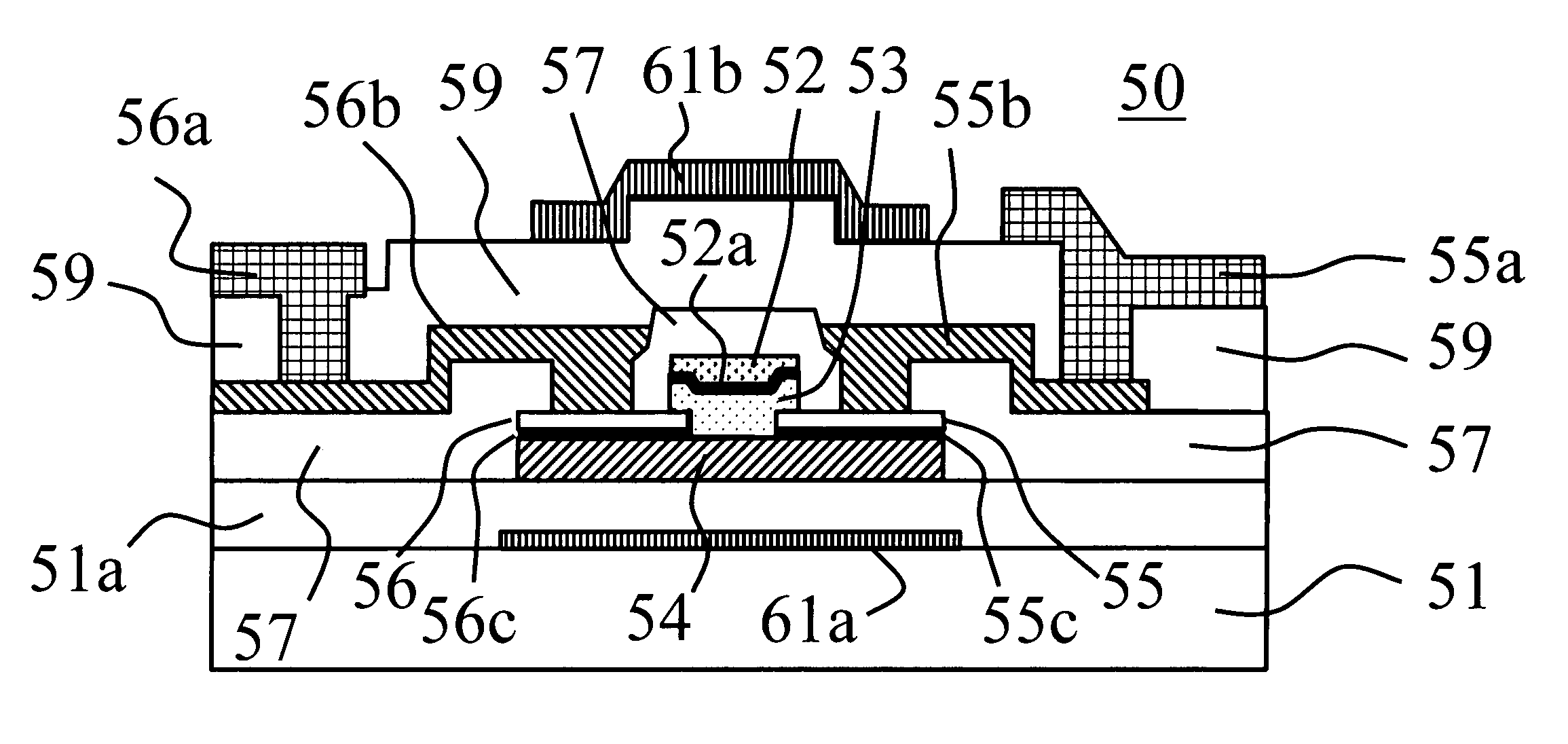
[0030]Indium oxide-based thin films have been developed over the last several decades as transparent and conducting oxide layers (TCO). Due to the large energy gaps (3.3–4.0 eV) and relatively large charge carrier mobilities, good thermal and chemical stabilities, the indium oxide-based thin films (notably indium tin oxide or commonly called ITO with an indium to tin ratio of 9:1) with very high electrical conductivities have been developed as the most important transparent and conducting oxide materials. These films have found various applications in electronic devices and circuits. In these devices and circuits, the ITO thin films deposited by various methods are used mainly as electrodes for conduction of electrical currents. For instance, ITO thin films are used as the bottom pixel electrodes and top electrodes in a liquid crystal display. From the above comments, it is clear that the material of ITO traditionally has been developed as transparent and conducting oxide layers (TC...


PUM


Abstract

In electronic displays or imaging units, the control of pixels is achieved by an array of transistors. These transistors are in a thin film form and arranged in a two-dimensional configuration to form switching circuits, driving circuits or even read-out circuits. In this invention, thin film transistors and circuits with indium oxide-based channel layers are provided. These thin film transistors and circuits may be fabricated at low temperatures on various substrates and with high charge carrier mobilities. In addition to conventional rigid substrates, the present thin film transistors and circuits are particularly suited for the fabrication on flexible and transparent substrates for electronic display and imaging applications. Methods for the fabrication of the thin film transistors with indium oxide-based channels are provided.

Description

FIELD OF INVENTION[0001]This invention relates to a family of indium oxide-based thin film transistors and a family of thin film transistor circuits for electronic signal, X-ray signal and optical signal processing and methods for fabricating the indium oxide-based thin film transistors and circuits.BACKGROUND OF THE INVENTION[0002]In circuits for electronic display and imaging applications, light emitting elements or light receiving elements are arranged either in one-dimensional or two-dimensional configurations to generate optical image patterns or to receive incident optical images. In order to generate image patterns, electrical signals from a circuit must be supplied to each light emitting element. In the case of electronic imaging units for receiving incident optical images, electrical signals from each light receiving element must be supplied to a circuit. FIG. 1 shows a simplified schematic diagram of a two-dimensional array (10). There are column electrical lines (11) each...

Claims


Application Information

Patent Timeline
Patent Type & Authority Patents(United States)
IPC IPC(8): H01L29/04H01L29/10H01L29/15H01L31/00H01L31/036H01L29/76H01L29/786
CPCH01L29/78633H01L29/78645H01L29/78648H01L29/7869
Inventor SHIH, YI-CHIQIU, CINDY XINGSHIH, ISHIANGQIU, CHUNONG
Owner SHIH YI CHI
Why Eureka
Try Eureka