Array substrate and method for manufacturing same

An array substrate and manufacturing method technology, applied in the field of liquid crystal display, can solve problems such as increased process difficulty, insufficient alignment accuracy, and product yield decline, and achieve the effects of reducing manufacturing costs, increasing aperture ratio, and simplifying structure

Active Publication Date: 2012-08-15
BOE TECH GRP CO LTD
View PDF6 Cites 51 Cited by
  • Summary
  • Abstract
  • Description
  • Claims
  • Application Information

AI Technical Summary

Problems solved by technology

Multiple mask exposures increase the difficulty of the process, which is prone to defects caused by insufficient alignment accuracy, and the product yield rate drops

Method used


Image

  • Array substrate and method for manufacturing same
  • Array substrate and method for manufacturing same
  • Array substrate and method for manufacturing same

Examples


Embodiment Construction

[0040] The specific implementation manners of the present invention will be further described in detail below in conjunction with the accompanying drawings and embodiments. The following examples are used to illustrate the present invention, but are not intended to limit the scope of the present invention.

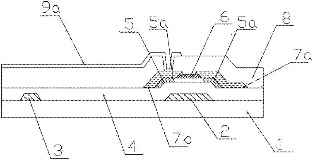
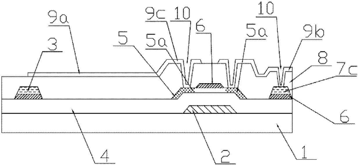
[0041] This embodiment provides an array substrate, including a substrate, a thin film transistor formed on the substrate, and a pixel electrode formed on the substrate, wherein the source and / or drain of the thin film transistor are made of a transparent conductive material. The thin film transistor may be a bottom gate type or a top gate type.

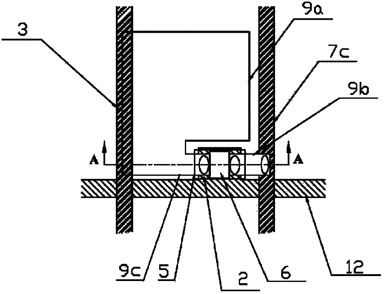
[0042] figure 2 It is a partial plan view (one of them) of a single pixel of the array substrate in this embodiment. On the transparent substrate 1, there are gate lines 12 and data lines 7c arranged vertically and intersecting each other, and a thin film transistor is arranged near the intersection point. The gate line 12 has...


PUM


Abstract

The invention belongs to the technical field of liquid crystal display, and particularly relates to an array substrate and a method for manufacturing the same. The oxide film transistor array substrate is provided with a source electrode and/or a drain electrode made of transparent conductive materials, a thin film transistor structure is simplified, and the aperture opening of a liquid crystal display device using the array substrate is increased. A common electrode wire and a data line are arranged on the same layer, the distance between the common electrode wire and a pixel electrode is shortened, storage capacitance is increased, and the performance of the array substrate is improved. When the array substrate is manufactured, by the aid of a half gray-level mask multi-step etching method, an etching protective film and the data line are obtained by means of mask exposure once, only five times of mask exposure are needed during manufacture of the array substrate, the process is simplified, and the manufacturing cost is reduced.

Description

technical field [0001] The invention belongs to the technical field of liquid crystal display, and in particular relates to an array substrate and a manufacturing method thereof. Background technique [0002] In the field of liquid crystal display, silicon-based materials with excellent stability and processability have been used in the active layer of thin-film transistors (TFT). Silicon-based materials are mainly divided into amorphous silicon and polycrystalline silicon, and the mobility of amorphous silicon materials is very low. , while polysilicon materials have higher mobility, but the uniformity of devices manufactured with them is poor, the yield rate is low, and the unit price is high. Therefore, in recent years, the technology of using transparent oxide semiconductors as active layer materials to manufacture thin film transistors and to apply them to electronic devices and optical devices has attracted extensive attention. The widely used oxide semiconductor mate...

Claims


Application Information

Patent Timeline
Patent Type & Authority Applications(China)
IPC IPC(8): G02F1/1362G02F1/1368H01L21/77
Inventor 牛菁
Owner BOE TECH GRP CO LTD
Why Eureka
Try Eureka