UV-Curing Apparatus Provided With Wavelength-Tuned Excimer Lamp and Method of Processing Semiconductor Substrate Using Same

a technology of excimer lamp and uv light, which is applied in the direction of measurement devices, instruments, scientific instruments, etc., can solve the problems of large drop in film density, difficult to obtain the required wavelength at the required illuminance, and the electrical characteristics of the device to be slightly deteriorated, so as to prevent unnecessary rise in semiconductor substrate/apparatus temperature, the effect of reducing cost and instant energy production

Inactive Publication Date: 2014-04-10
ASM IP HLDG BV
View PDF12 Cites 366 Cited by
  • Summary
  • Abstract
  • Description
  • Claims
  • Application Information

AI Technical Summary

Benefits of technology

[0011]In an embodiment of the present invention, the UV luminous tube is a dielectric barrier discharge excimer lamp with rare gas charged inside, which has a peak spectrum in a wavelength range of 190 to 350 nm depending on the type of the fluorescent substance applied to the interior walls of the UV luminous tube. In other words, use of a dielectric barrier discharge excimer lamp being a Xe excimer lamp allows for output of any desired wavelength in a range of 172 nm or more (190 to 350 nm) to permit tuning of wavelengths to one effective for the process. There are no wavelengths corresponding to the heat ray range, which prevents unnecessary rise in semiconductor substrate / apparatus temperatures and keeps the process stable, and because no cooling mechanism is required and a low-output power supply can be used, the cost can be reduced. Furthermore, this lamp becomes stable quickly after it is turned on, unlike the conventional mercury lamp, and required energy can be produced instantly, and also this lamp can be used in flashing mode and steady irradiation mode, which eliminates the need for a shutter and allows the structure to be simplified.

Problems solved by technology

However, if a UV luminous tube is a dielectric barrier discharge excimer lamp, it is difficult to obtain the required wavelength at the required illuminance.
However, sizes of voids formed in the film as a result of irradiation are small on average but widely distributed, and some voids are large in size, which results in a large rate of drop in film density.
It is also found that presence of Si—H bonds in the film cause the electrical characteristics of the device to slightly deteriorate.
However, a 172-nm Xe excimer lamp generating high energy presents problems, such as negatively affecting the chemical bonding of quartz and causing the transmittance to drop.
However, use of a high-pressure mercury lamp presents problems, such as the generation of heat due to unnecessary wavelengths which are not optimal for the process account for a majority of the overall output, which causes the temperature of the semiconductor substrate to rise significantly, or by approx.
20° C., and also requires large attached equipment including a power supply and cooling mechanism to support such large output and control the heat, leading to higher cost and a larger footprint.

Method used


Image

  • UV-Curing Apparatus Provided With Wavelength-Tuned Excimer Lamp and Method of Processing Semiconductor Substrate Using Same
  • UV-Curing Apparatus Provided With Wavelength-Tuned Excimer Lamp and Method of Processing Semiconductor Substrate Using Same
  • UV-Curing Apparatus Provided With Wavelength-Tuned Excimer Lamp and Method of Processing Semiconductor Substrate Using Same

Examples


examples 1 to 6

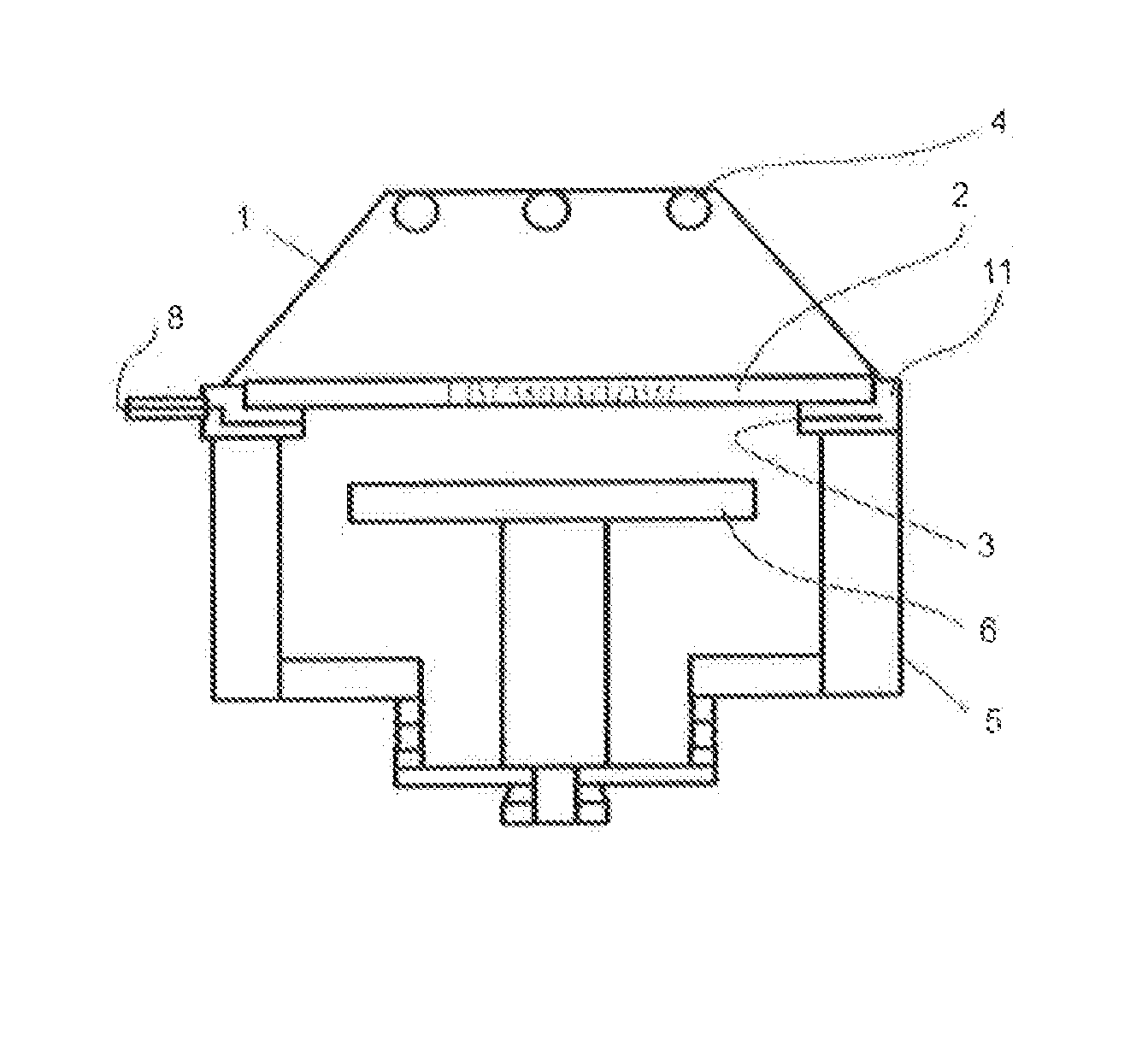
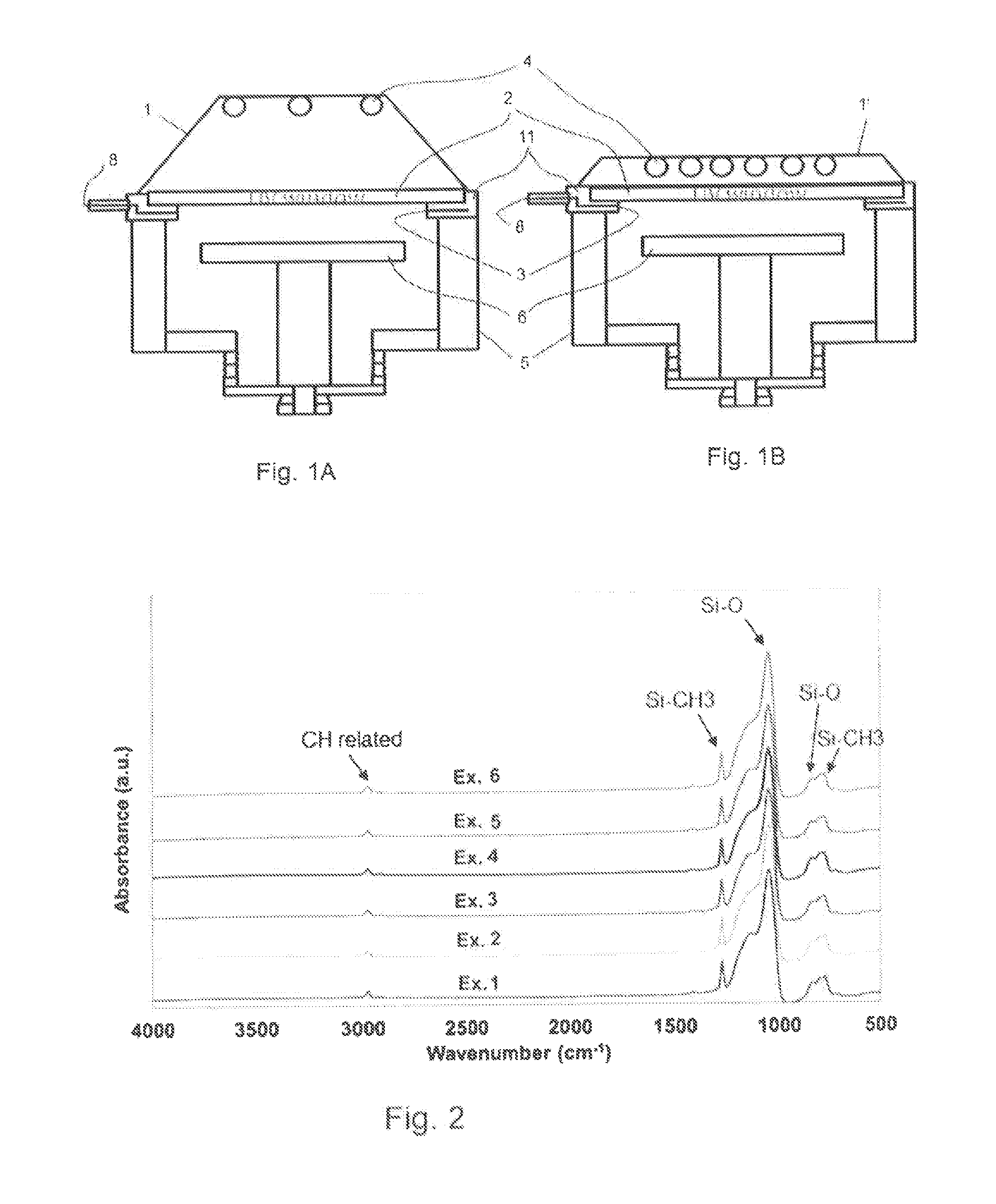
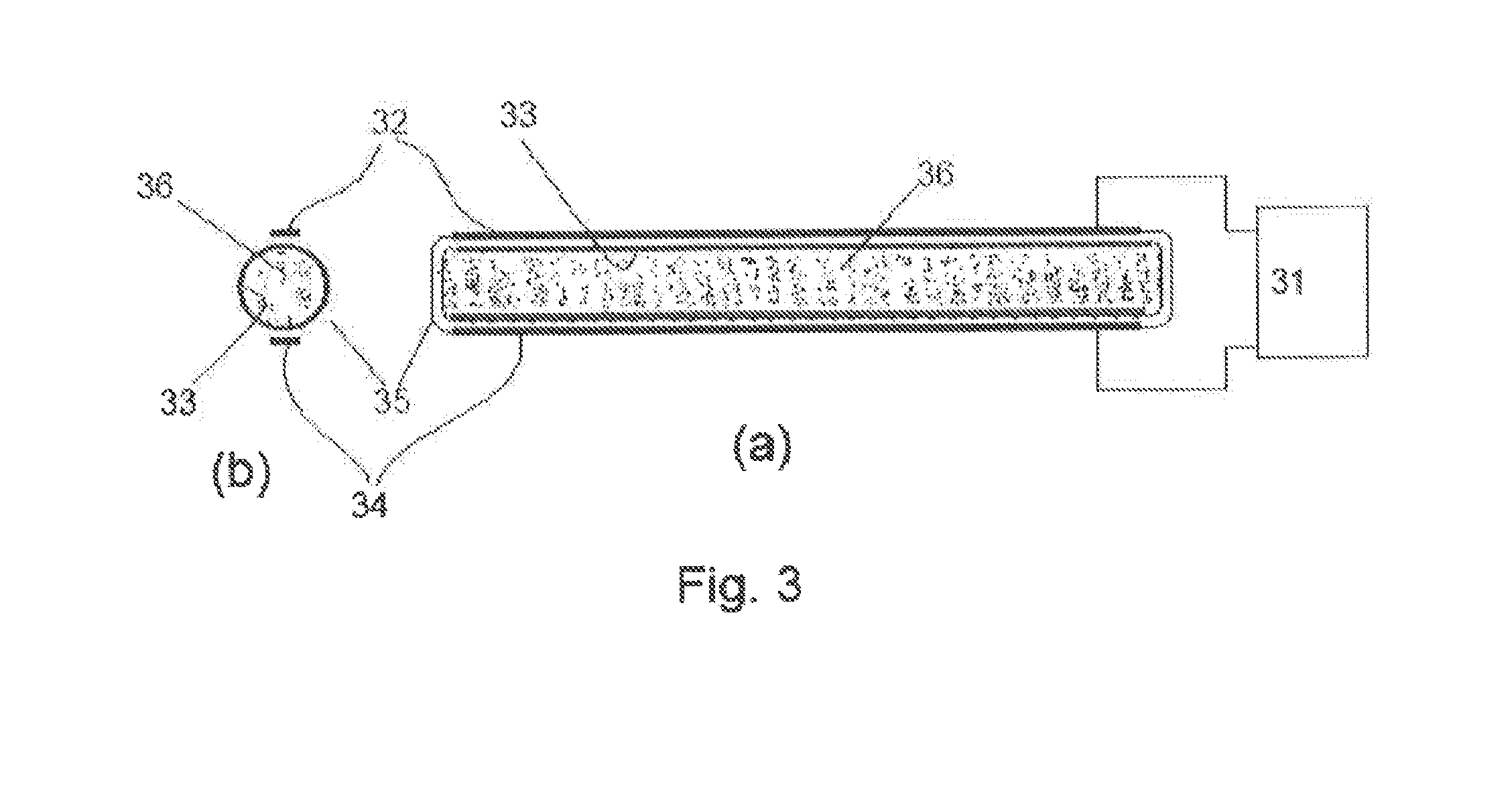
[0045]A substrate (300 mm in diameter) having a dielectric film containing a porogen material formed thereon was loaded in a UV irradiation apparatus illustrated in FIG. 1B wherein dielectric barrier discharge excimer lamps illustrated in FIG. 3 were installed. The tubes of the lamps contained Xe gas, and the fluorescent substances applied on an inner surface of the tubes are shown in Table 2 below. Table 2 also shows alternatively usable fluorescent substances. No water-cooling system was used. The dielectric film formed on the substrate was cured in the apparatus using UV light emitted from the lamps under the following conditions:

[0046]Pressure: 5 Torr

[0047]Supplied gas: Nitrogen gas

[0048]Temperature: 400° C.

[0049]Distance between the substrate and the lamps: 100 mm

[0050]Power applied to the lamps: 4 W / cm2

[0051]Irradiation duration: 60 to 1,200 seconds

TABLE 2EmissionFluorescentpeak spectrumsubstanceAlternativeEx. 1190 nmLaPO4: NdYPO4: Nd, LuPO4: NdEx. 2230 nmLaPO4: PrCaSO4: PrEx...


PUM


Abstract

A UV irradiation apparatus for processing a semiconductor substrate includes: a UV lamp unit having at least one dielectric barrier discharge excimer lamp which is constituted by a luminous tube containing a rare gas wherein an inner surface of the luminous tube is coated with a fluorescent substance having a peak emission spectrum in a wavelength range of 190 nm to 350 nm; and a reaction chamber disposed under the UV lamp unit and connected thereto via a transmission window.

Description

BACKGROUND OF THE INVENTION[0001]1. Field of the Invention[0002]The present invention generally relates to a UV light irradiating apparatus and a method for irradiating a semiconductor substrate.[0003]2. Description of the Related Art[0004]In general, UV irradiation apparatuses have been used for the quality modification of various processing targets via ultraviolet light and preparation of substances using photochemical reaction. With the recent trend for higher integration of devices, which requires finer wiring designs and multi-layer wiring structures, it is essential to reduce the inter-layer capacitance to make the devices operate faster while consuming less power. Low-k (low dielectric constant film) materials are used to reduce the inter-layer capacitance, but these materials not only lower the dielectric constant, but also reduce the mechanical strength (EM: elastic modulus), and are vulnerable to stress received after the CMP, wire bonding, and packaging post-processes. On...

Claims


Application Information

Patent Timeline
Patent Type & Authority Applications(United States)
IPC IPC(8): H01L21/268
CPCH01L21/268H01L21/2686
Inventor TSUJI, NAOTO
Owner ASM IP HLDG BV
Why Eureka
Try Eureka