Thin-film device and method of fabricating the same

Active Publication Date: 2008-02-14
NEC LCD TECH CORP
View PDF18 Cites 4119 Cited by
  • Summary
  • Abstract
  • Description
  • Claims
  • Application Information

AI Technical Summary

Benefits of technology

[0016]In a second exemplary aspect of the present invention, there is provided a method of fabricating a thin-film device, including forming an oxide-semiconductor film on a first electrical insulator, forming a second electrical insulator on the oxide-semiconductor film, the oxide-semiconductor film defining an active layer, the oxide-semiconductor film being comprised of a first interface layer located at

Problems solved by technology

The above listed Publications are accompanied with a problem of insufficient control to oxygen holes existing at an interface layer.
This is because such annealing is difficult to penetrate an oxide-semiconductor film.
It may be possible to oxidize even a lower surface of an oxide-semiconductor film by carrying out annealing at 600 degrees centigrade or higher for enhancing penetration of oxidation, however, in which case, there would be caused problems that it is not possible to use a cheap glass substrate as an ele

Method used


Image

  • Thin-film device and method of fabricating the same
  • Thin-film device and method of fabricating the same
  • Thin-film device and method of fabricating the same

Examples


first exemplary embodiment

[0050]FIGS. 1 to 8 are cross-sectional views of a thin-film device 100, each showing a step to be carried out in a method of fabricating a thin-film device 100 in accordance with the first exemplary embodiment.

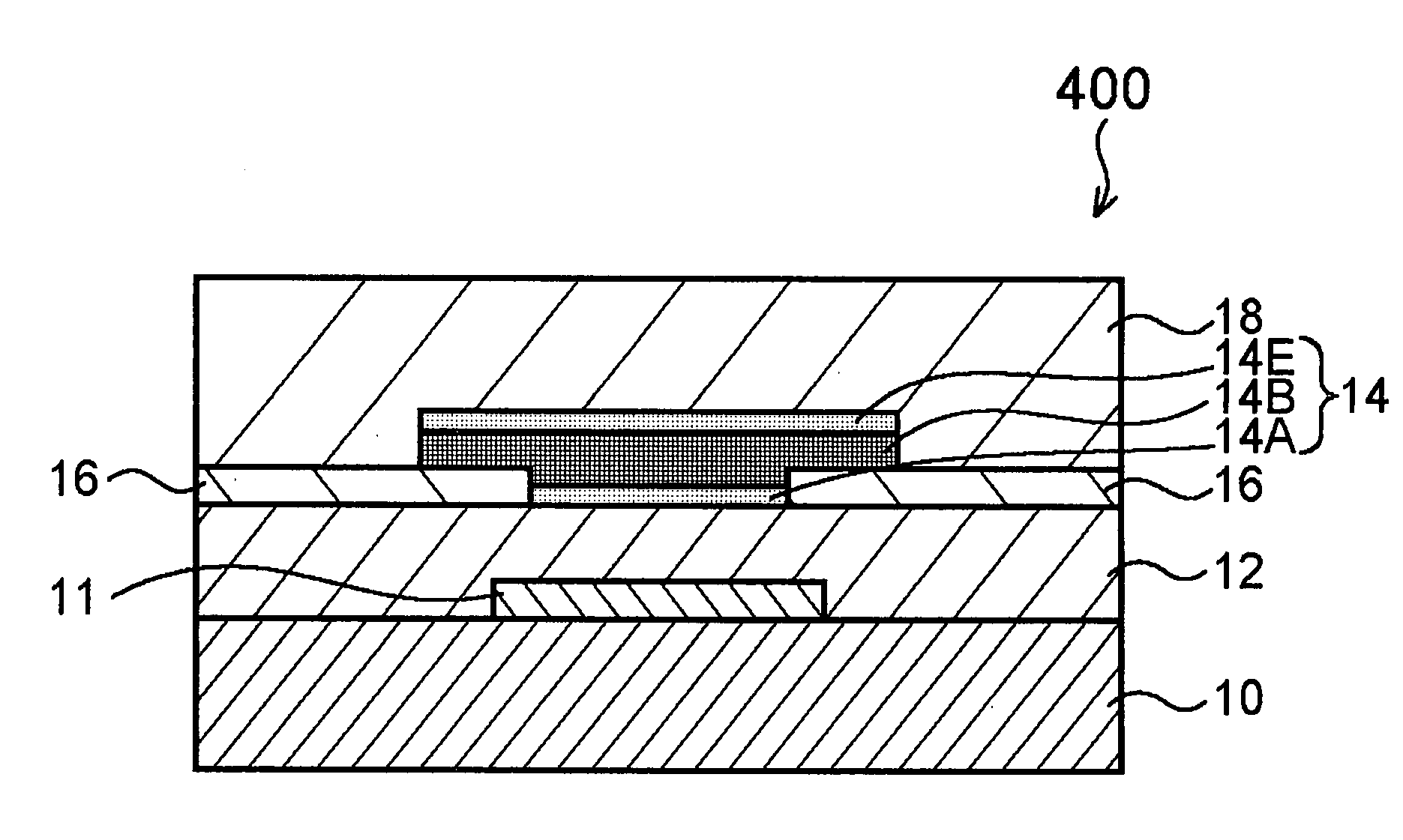
[0051]A thin-film device 100 in the first exemplary embodiment is comprised of a bottom gate stagger type thin-film transistor.

[0052]Hereinbelow is explained a method of fabricating the thin-film device 100.

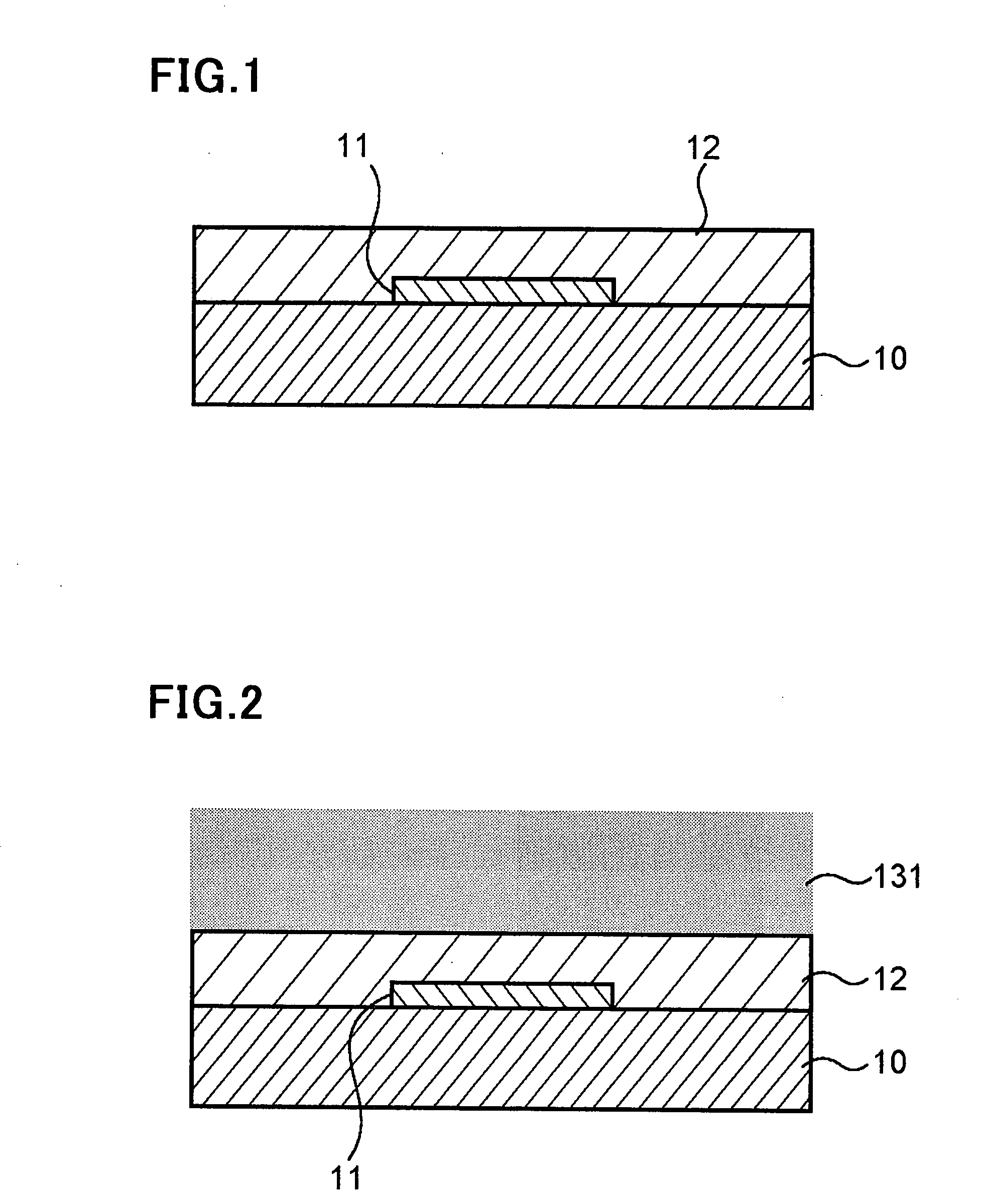
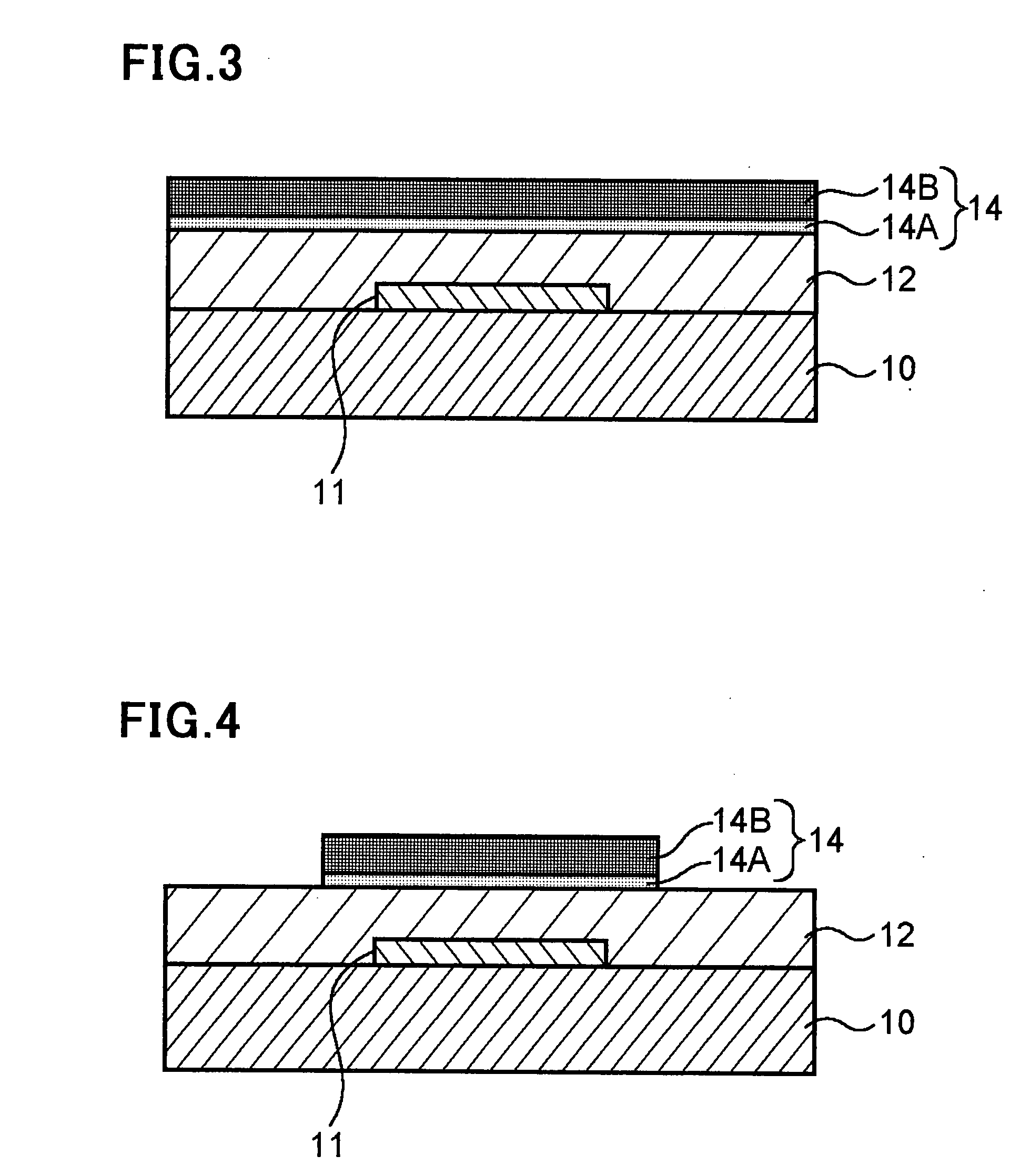
[0053]First, as illustrated in FIG. 1, a gate metal film is formed on an electrically insulating substrate 10, and then, the gate metal film is patterned into a gate electrode 11.

[0054]Then, a gate insulating film 12 as a first electrical insulator is formed on the electrically insulating substrate 10 so as to cover the gate electrode 11 therewith.

[0055]Then, as illustrated in FIG. 2, first oxidation 131 is applied to the gate insulating film 12 without exposing a device (that is, the electrically insulating substrate 10, the gate electrode 11, and the gate insulating film ...

second exemplary embodiment

[0089]FIGS. 9 to 14 are cross-sectional views of a thin-film device 200, each showing a step to be carried out in a method of fabricating a thin-film device 200 in accordance with the second exemplary embodiment.

[0090]A thin-film device 200 in the second exemplary embodiment is comprised of a top gate stagger type thin-film transistor.

[0091]Hereinbelow is explained a method of fabricating the thin-film device 200.

[0092]As illustrated in FIG. 9, an underlying insulating film (first electrical insulator) 21 is formed on an electrically insulating substrate 10. Then, a source / drain metal film is formed on the underlying insulating film 21, and subsequently, the source / drain metal film is patterned into source and drain electrodes 16 (one of which is a source electrode, and the other is a drain electrode).

[0093]Then, as illustrated in FIG. 10, first oxidation 131 is applied to the underlying insulating film 21.

[0094]The first oxidation 131 is comprised of application of oxygen plasma, f...

third exemplary embodiment

[0111]FIGS. 15 to 19 are cross-sectional views of a thin-film device 300, each showing a step to be carried out in a method of fabricating a thin-film device 300 in accordance with the third exemplary embodiment.

[0112]A thin-film device 300 in the third exemplary embodiment is comprised of a top gate planar type thin-film transistor.

[0113]Hereinbelow is explained a method of fabricating the thin-film device 300.

[0114]First, as illustrated in FIG. 15, an underlying insulating film 21 as a first electrical insulator is formed on an electrically insulating substrate 10.

[0115]Then, first oxidation 131 is applied to the underlying insulating film 21.

[0116]The first oxidation 131 is comprised of application of oxygen plasma, for instance.

[0117]Then, as illustrated in FIG. 16, an oxide-semiconductor film 14 is formed on the underlying insulating film 21 without exposing to atmosphere.

[0118]The first oxidation 131 causes oxygen to be adhered to a surface of the underlying insulating film 21...


PUM


Abstract

A thin-film device includes a first electrical insulator, an oxide-semiconductor film formed on the first electrical insulator, and a second electrical insulator formed on the oxide-semiconductor film, the oxide-semiconductor film defining an active layer. The oxide-semiconductor film is comprised of a first interface layer located at an interface with the first electrical insulating insulator, a second interface layer located at an interface with the second electrical insulator, and a bulk layer other than the first and second interface layers. A density of oxygen holes in at least one of the first and second interlayer layers is smaller than a density of oxygen holes in the bulk layer.

Description

BACKGROUND OF THE INVENTION[0001]1. Field of the Invention[0002]The invention relates to a thin-film device, and a method of fabricating the same.[0003]2. Description of the Related Art[0004]A transparent electrically conductive film composed of oxide, such as an ITO film composed of compound of indium (In), tin (Sn), and oxygen (O), is frequently used in a flat panel display or a photoelectric transfer device, since it has a sheet resistance of a few ohms per a unit area even if it has a small thickness such as hundreds of nanometers, and it has high transmittance to visible light.[0005]Furthermore, a study to a thin-film transistor including a channel layer composed of transparent oxide semiconductor such as In—Ga—Zn—O has been recently started. Such oxide semiconductor contains highly ionic bonds, and is characterized by a small difference in electron mobility between crystalline state and amorphous state. Accordingly, relatively high electron mobility can be obtained even in amo...

Claims


Application Information

Patent Timeline
IPC IPC(8): H01L21/84H01L29/02
CPCH01L29/4908H01L29/7869H01L29/66969H01L21/02694H01L29/78696H01L21/02554H01L21/02587H01L29/78618
Inventor TAKECHI, KAZUSHIGENAKATA, MITSURU
Owner NEC LCD TECH CORP
Why Eureka
Try Eureka