Light-emitting device

Active Publication Date: 2006-06-01
CANON KK +2
View PDF11 Cites 4055 Cited by
  • Summary
  • Abstract
  • Description
  • Claims
  • Application Information

AI Technical Summary

Benefits of technology

[0027] the active layer of the field effect transistor includes such a transparent amorphous-oxide semiconductor as to be capable of realizing a normally off state. The transparent amorphous-oxide semiconductor preferably has an electronic carrier concentration of less than 1018/cm3, which is sufficiently few in realizing the normally off state.
[0028] According to a fur

Problems solved by technology

However, because a thermal process in a comparatively high temperature is necessary to manufacture a transistor with the use of the above described silicon thin film, it is difficult to directly form the silicon thin film on a resin substrate with low

Method used


Image

  • Light-emitting device
  • Light-emitting device
  • Light-emitting device

Examples


second embodiment

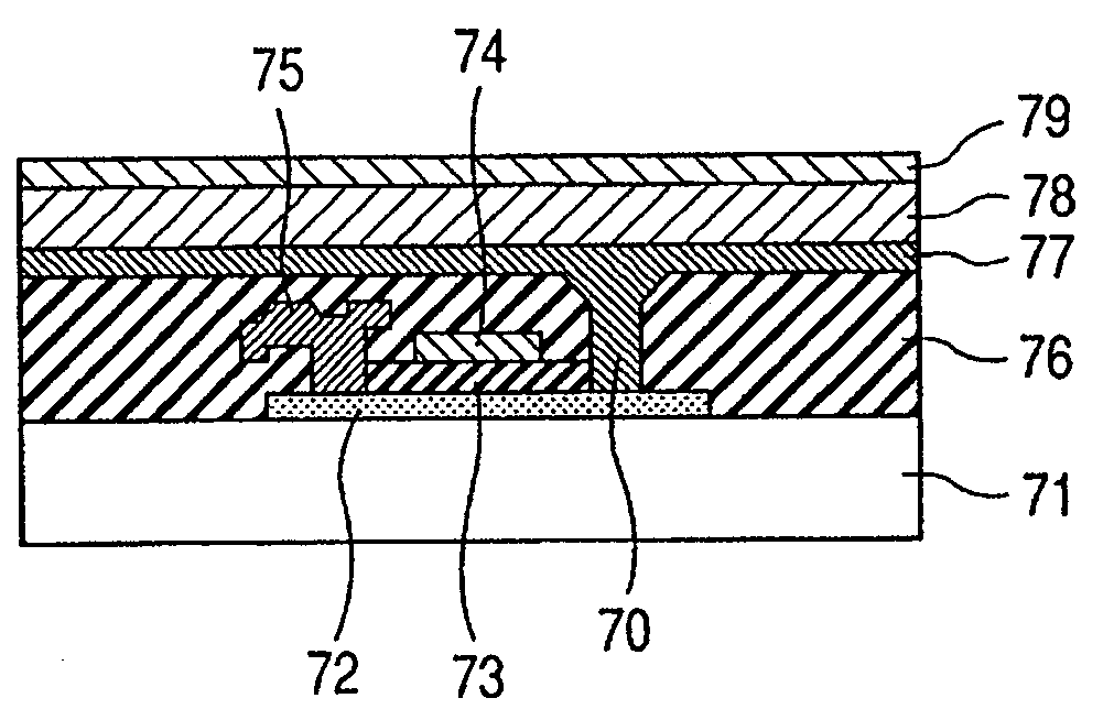
[0107] In FIG. 9, reference numeral 91 denotes a substrate, reference numeral 92 an active layer made of a semiconductor material peculiar to the present invention, reference numeral 93 a gate insulation film, reference numeral 94 a gate electrode, reference numeral 95 a source electrode, reference numeral 96 an insulation layer, and reference numeral 97 a bottom electrode. The bottom electrode 97 is layered on a drain electrode or is identical to the drain electrode, in other words, is the drain electrode in itself. Reference numeral 98 denotes an organic EL layer, and reference numeral 99 a counter electrode.

[0108] The present embodiment has basically the same type of configuration in the first embodiment in which a part of a bottom electrode contacts with a drain electrode through wiring, but has a different configuration in which the drain electrode and a light-emitting layer are layered on the same overlapping area when viewed from the position above a substrate 91, and the bo...

third embodiment

[0117] In FIG. 8, reference numeral 81 denotes a transistor for driving an organic EL layer 84, which passes a current to a light-emitting element that has the organic EL layer 84 and a pair of electrodes sandwiching the organic EL layer 84. Reference numeral 82 is a transistor 2 for selecting a picture element, which supplies a picture signal for determining a current to be passed to the light-emitting element, to a gate of the transistor 81.

[0118] In addition, a condenser 83 is placed in order to hold a selected condition, stores electrical charges between a common electrode wire 87 and a source electrode part of the transistor 2, and retains the signal of the gate of the transistor 1. The picture element is selected and determined by a scan electrode wire 85 and a signal electrode wire 86.

[0119] The configuration will be now more specifically described.

[0120] At the same time when a row selection signal is applied to a gate electrode from a driver circuit (not shown) through a...

fourth embodiment

[0124] A fourth embodiment according to the present invention is a bottom emission type of a light-emitting device as shown in FIGS. 11 and 12.

[0125] Specifically, the light-emitting device has the above described light-emitting layer and the above described field effect transistor arranged on an optically transparent substrate, and emits light from the above described light-emitting layer through the above described substrate. In FIG. 11, an active layer (a channel layer 2101) formed of an amorphous oxide arranged also right under a light-emitting element 2160, but needs not to be arranged right under it. As a matter of course, in a configuration of FIG. 11, light emitted from the light-emitting layer 2108 passes through the active layer formed of the above described amorphous oxide and the substrate 2100.

[0126] By the way, a light source can be produced by disposing a light-emitting device according to the present invention in one dimension, and can make an apparatus by combinin...


PUM


Abstract

An object of the present invention is to provide a new light-emitting device with the use of an amorphous oxide. The light-emitting device has a light-emitting layer existing between first and second electrodes and a field effect transistor, of which the active layer is an amorphous.

Description

BACKGROUND OF THE INVENTION [0001] 1. Field of the Invention [0002] The present invention relates to a light-emitting device using an oxide, and particularly using an organic EL element and an inorganic EL element. The light-emitting device according to the present invention also relates to a top emission type or a bottom emission type. [0003] 2. Related Background Art [0004] In recent years, a flat panel display (FPD) is in practical use as a result of the progress of technologies relating to a liquid crystal and electroluminescence (EL). The FPD is driven by an active matrix circuit consisting of a field effect thin film transistor (TFT) using an amorphous silicon thin film or a polycrystalline silicon thin film provided on a glass substrate as an active layer. [0005] On the other hand, an attempt has been made to use a lightweight and flexible resin substrate in place of the glass substrate, in quest of further improvement in thinning, slimming and breakage resistance of an FPD. ...

Claims


Application Information

Patent Timeline
IPC IPC(8): H01L33/00H01L31/12B41J2/44B41J2/45B41J2/455G09F9/30H01L27/32H01L29/786H01L51/50H05B33/10
CPCG03G5/08G03G5/144H01L27/1214H01L27/3248H01L27/3262H01L29/04H01L29/7869H01L2251/5315H01L29/66969H01L29/78693H01L27/1225H10K59/123H10K59/1213H10K2102/3026H01L21/02592H01L29/1025H01L29/41725
Inventor DEN, TOHRUIWASAKI, TATSUYAHOSONO, HIDEOKAMIYA, TOSHIONOMURA, KENJI
Owner CANON KK
Why Eureka
Try Eureka