

Display
- Summary
- Abstract
- Description
- Claims
- Application Information
AI Technical Summary
Benefits of technology
Problems solved by technology
Method used
Image

Examples
first embodiment
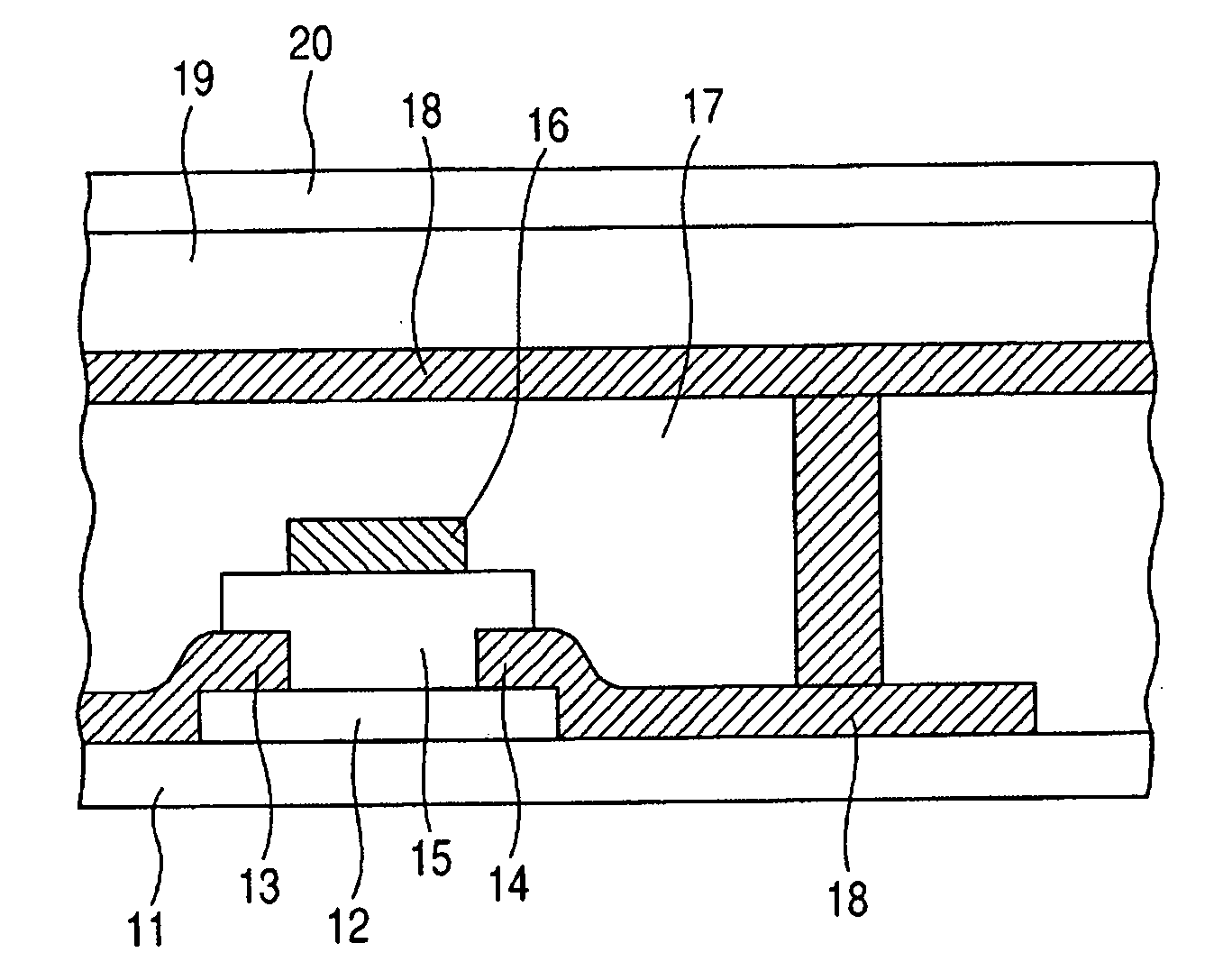
[0076] The active matrix display according to the present invention will be described with reference to FIG. 8.
[0077] In the figure, reference numeral 11 denotes a base substance or substrate; 12, an amorphous oxide; 13, a source electrode; 14, a drain electrode; 18, an electrode (pixel electrode); 15, a gate insulation film; 16, a gate electrode; 21 and 22, high-resistance films; and 23, a portion containing a liquid crystal or an electrophoretic particle. The portion 23 constitutes part of the light control device in the present invention. Reference numeral 20 denotes an electrode or a substrate having an electrode. An example of the electrode includes a transparent electrode such as ITO.
[0078] In the present invention, an output terminal (corresponding to the drain electrode 14) of a field effect transistor for driving the light control device constituted by a liquid crystal or the like is connected to the electrode 18 constituting the light control device.
[0079] The light con...
second embodiment
[0297] The present invention also relates to a light control device obtained by connecting, to a drain as an output terminal of a field effect TFT, an input electrode of a light-emitting device such as an electroluminescent device; or a light transmittance control device or a light reflectance control device composed of a liquid crystal cell or an electrophoretic particle cell.
[0298] Description will be made with reference to FIG. 7.
[0299] A TFT is constituted by an amorphous oxide semiconductor film 12 deposited and patterned on a substrate 11, a source electrode 13, a drain electrode 14, a gate insulation film 15, and a gate electrode 16.
[0300] An electrode 18 is connected to the drain electrode 14 via an interlayer insulation film 17. The electrode 18 is in contact with a light-emitting layer 19, and the light-emitting layer 19 is in contact with an electrode 20.
[0301] A current to be injected into the light-emitting layer 19 is controlled on the basis of the value for a curr...
example 1
Production of Light Control Device Using the Above TFT
[0338] In the above TFT, a shorter side of the island composed of an ITO film to serve as the drain electrode is extended up to 100 μm. The extended 90-μm portion is left, and the TFT is coated with an insulating layer with wiring to the source electrode and the gate electrode secured.
[0339] A polyimide film (orientation film) is applied to the layer to perform a rubbing step.
[0340] Meanwhile, a plastic substrate having an ITO film and a polyimide film formed thereon and subjected to a rubbing step is separately prepared. The above substrate on which the TFT has been formed and the separately prepared substrate are arranged so as to be opposite to each other with a gap of 5 μm between them. A nematic liquid crystal is injected into the gap.
[0341] Furthermore, a pair of polarizing plates are arranged on both sides of the structure.
[0342] Here, when a voltage is applied to the source electrode of the TFT and the voltage applie...
PUM
 Abstract
Description
Claims
Application Information