Stabilized active matrix emissive display

a technology of emissive display and active matrix, which is applied in the direction of lighting apparatus, instruments, light sources, etc., can solve the problems of high level of uniformity, difficult production and/or maintenance in the thin film area, and often the problem of uniformity in the emissive display

Inactive Publication Date: 2005-11-10
LEADIS TECH
View PDF66 Cites 187 Cited by
  • Summary
  • Abstract
  • Description
  • Claims
  • Application Information

AI Technical Summary

Benefits of technology

[0009] In some embodiments, the ramp voltage is generated within each pixel, thereby eliminating the need of a separate conductive line to connect each line of pixels to a ramp voltage supply. In further embodiments, an optical sensor is provided for each pixel to provide a feedback measure for the pixel luminance. The feedback measure is provided to a control circuit via a conductive line associated with a column of pixels, which also connects a control gate of each switching device in the column of pixels to the control circuit. The control circuit is configured to turn off the switching device in response to the feedback measure having reached a reference level corresponding to the specified luminance of the pixel.

Problems solved by technology

Therefore, uniformity in an emissive display is often a problem.
Such high level of uniformity, however, is often difficult to produce and / or to maintain in the thin film area.
In addition to the uniformity problem, active matrix emissive displays often are designed in a manner that they consume excessive amounts of power.

Method used


Image

  • Stabilized active matrix emissive display
  • Stabilized active matrix emissive display
  • Stabilized active matrix emissive display

Examples


Embodiment Construction

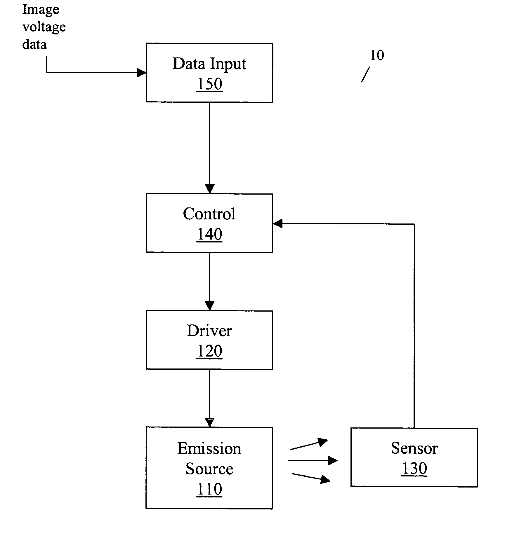
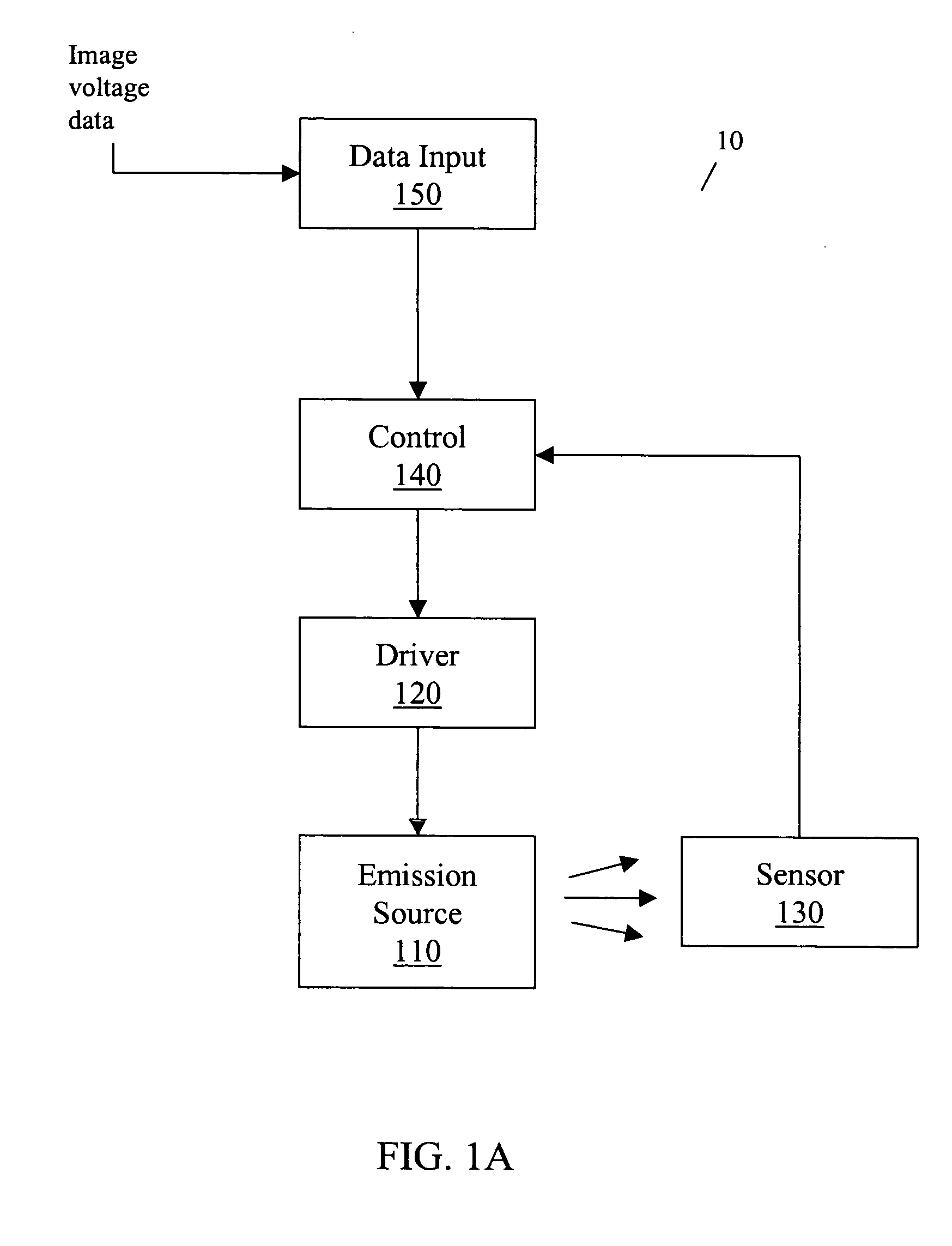
[0018] Embodiments of the present invention provide improved stabilized emissive displays and methods of operating the same. The embodiments described herein improve reliability and reduce costs associated with manufacturing the displays by providing a display circuitry with reduced number of conducting lines interconnecting the pixels in the displays to control circuits.

[0019]FIG. 1A is a block diagram of a portion of an exemplary emissive feedback display, such as a flat panel display, a display circuit 10 according to one embodiment of the present invention. As shown in FIG. 1A, display circuit 10 comprises a light emission source 110, an emission driver 120 configured to vary the luminance of the emission source 110, an optical sensor 130 positioned to receive a portion of the light emitted from emission source 110 and having an associated electrical parameter dependent on the received light, a control unit 140 configured to control the driver 120 based on the changes in the el...


PUM


Abstract

The embodiments of the present invention provide a flat panel display having a plurality of pixels, each comprising a light-emitting device configured to emit light in accordance with a current flowing through the light-emitting device, a transistor coupled to the light-emitting device and configured to provide the current through the light-emitting device, the current increasing with a ramp voltage applied to a control terminal of the transistor, and a switching device configured to switch off in response to the luminance of the light-emitting device having reached a specified level, thereby disconnecting the ramp voltage from the transistor and locking the brightness at the specified level. The ramp voltage is generated in each pixel instead of in peripheral circuits, thereby reducing the number of conducting lines in the display.

Description

CROSS REFERENCE TO RELATED APPLICATIONS [0001] The present application claims benefit of and priority under 35 U.S.C. 119 and / or 35 U.S.C. 120 to U.S. Provisional Patent Application No. 60 / 566,191 entitled “Stabilized Flat Panel Display,” filed on Apr. 28, 2004, the entire disclosure of which is incorporated herein by reference.FIELD OF THE INVENTION [0002] The present invention relates to active matrix emissive displays and particularly to an improved stabilized active matrix emissive display and method of operating the same. BACKGROUND OF THE INVENTION [0003] A flat panel display (FPD) typically includes an array of picture elements (or pixels). Image data for the pixels is converted into electrical signals, which are fed to the pixels to control either the amount of backlight passed by the pixels as in a liquid crystal display (LCD), or to cause the pixels to emit specified amount of light as in, for example, an electro-luminescent LCD display, or an organic light emitting diode ...

Claims


Application Information

Patent Timeline
Patent Type & Authority Applications(United States)
IPC IPC(8): G09G3/30G09G3/32
CPCG09G3/3233G09G3/3291G09G2300/0842G09G2310/0259G09G2310/027G09G2360/148G09G2320/0295G09G2320/043G09G2330/021G09G2360/147G09G2310/066G09G3/30G09G3/32H05B33/14G09G3/20
Inventor NAUGLER, W. EDWARD JR.REDDY, DAMODER
Owner LEADIS TECH
Why Eureka
Try Eureka