Method for forming ZnO film, method for forming ZnO semiconductor layer, method for fabricating semiconductor device, and semiconductor device

a technology of zno film and zno semiconductor layer, which is applied in the direction of crystal growth process, crystal growth process, polycrystalline material growth, etc., can solve the problems of increased fabrication cost, increased apparatus cost, and increased fabrication cost, and achieves good crystallinity and low cost.

Inactive Publication Date: 2006-05-23
SANYO ELECTRIC CO LTD
View PDF7 Cites 4037 Cited by
  • Summary
  • Abstract
  • Description
  • Claims
  • Application Information

AI Technical Summary

Benefits of technology

[0009]The invention has been devised with considering such a situation. An object of the invention is to provide a method for forming a ZnO semiconductor layer having good crystallinity at a low cost.
[0010]Another object of the invention is to provide a method for fabricating a semiconductor device comprising a ZnO semiconductor layer having good crystallinity at a low cost.
[0011]Further another object of the invention is to provide a semiconductor device comprising a ZnO semiconductor layer having good crystallinity.

Problems solved by technology

This causes the problem of an increase in the fabrication cost.
Nevertheless, this causes the problem of an increase in the apparatus cost and, hence, in the fabrication cost.
This causes the problem of an increase in the necessary process time and, hence, in the fabrication cost.
Nevertheless, this causes similarly the problem of an increase in the apparatus cost and, hence, in the fabrication cost.
This causes an increase in the material cost or in the number of fabrication processes, and thereby results in the problem of a higher cost of the electronic devices.

Method used


Image

  • Method for forming ZnO film, method for forming ZnO semiconductor layer, method for fabricating semiconductor device, and semiconductor device
  • Method for forming ZnO film, method for forming ZnO semiconductor layer, method for fabricating semiconductor device, and semiconductor device
  • Method for forming ZnO film, method for forming ZnO semiconductor layer, method for fabricating semiconductor device, and semiconductor device

Examples


example 1

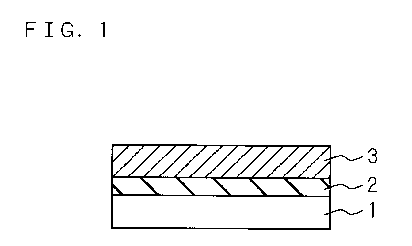
[0077]In Example 1, a ZnO buffer layer 2 and a ZnO semiconductor layer 3 were formed on a glass substrate 1 by sputtering under the condition shown in Table 3.

[0078]

TABLE 3SubstrateRFAr FlowO2 FlowThick-TemperaturePowerPressureRateRateness(° C.)(W)(Pa)(sccm)(sccm)(nm)Buffer3001000.60~150~15500Layeror800Semi-3001000.6150200conductorLayer*In formation of buffer layer, Ar flow rate + O2 flow rate = 15 sccm

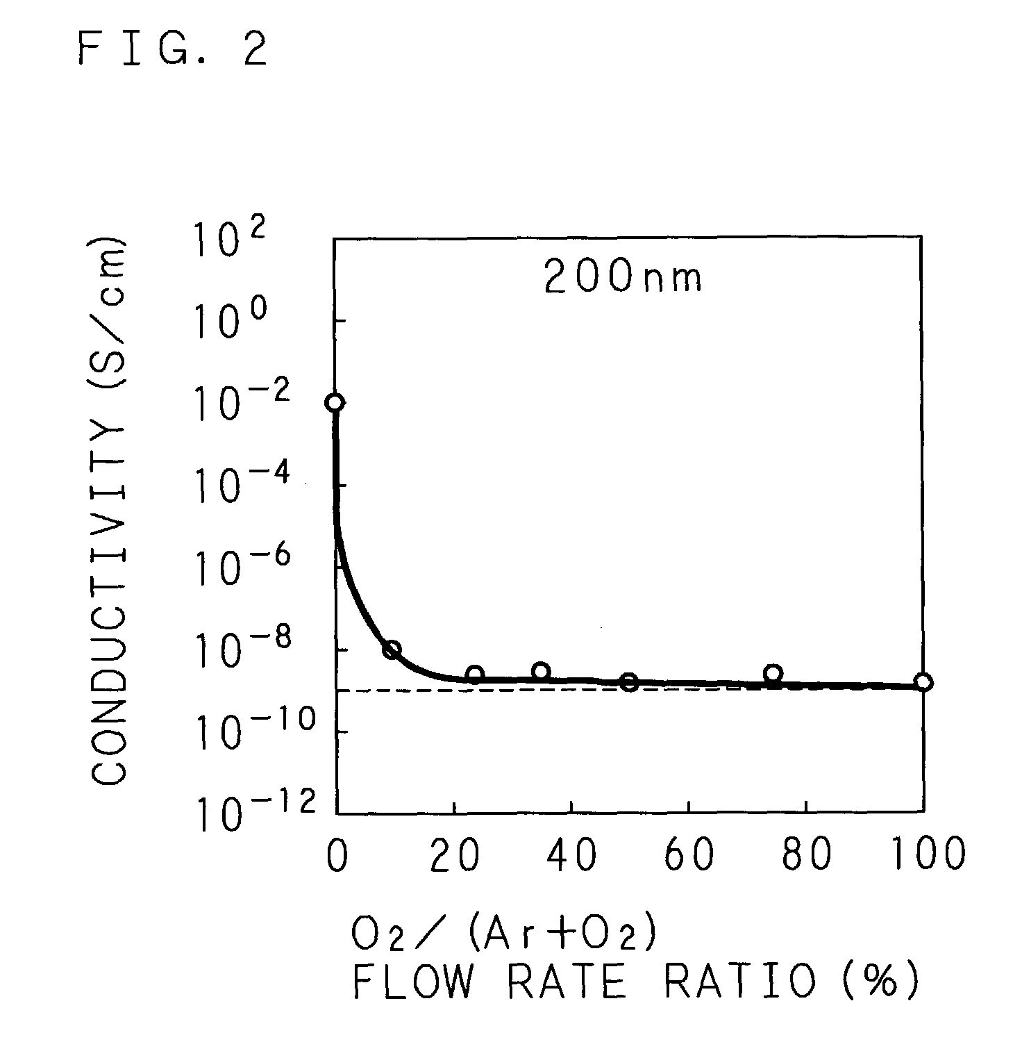
[0079]The ZnO buffer layer 2 and the ZnO semiconductor layer 3 were formed successively in the same sputtering chamber by maintaining the substrate temperature at constant at 300° C. and by changing the sputtering gas without stopping the electric discharge. In the formation of the ZnO buffer layer 2, plural kinds of ZnO buffer layers 2 were formed using a mixture gas between Ar gas and O2 gas as the sputtering gas, at a constant total flow rate of the sputtering gas of 15 sccm, at various flow rate ratios of the oxygen gas of 25%, 50%, and 100%, into various film thickness values of ...

example 2

[0090]In Example 2, a ZnO buffer layer 2 and a ZnO semiconductor layer 3 were formed on a glass substrate 1 by sputtering under the condition shown in Table 5. The mobility and the carrier density of the obtained stacked film were measured by Hall effect measurement.

[0091]

TABLE 5SubstrateRFAr FlowO2 FlowThick-TemperaturePowerPressureRateRateness(° C.)(W)(Pa)(sccm)(sccm)(nm)Buffer3001000.6015100~Layer2000Semi-3001000.6150 200conductorLayer

[0092]The difference of Example 2 from Example 1 was that the flow rate ratio of the oxygen gas in the sputtering gas was maintained constant at 100% during the formation of the ZnO buffer layer 2 and that the film thickness of the ZnO buffer layer 2 was changed in a range from 100 nm to 2000 nm. FIG. 17 shows the relation between the mobility of the stacked film composed of ZnO buffer layer 2 / ZnO semiconductor layer 3 and the film thickness of the ZnO buffer layer 2. FIG. 18 shows the relation between the carrier density in the stacked film and the...

example 3

[0109]In an example of the present embodiment, a ZnO buffer layer 12 and a ZnO semiconductor layer 13 were formed under the condition shown in Table 6, whereby a TFT was fabricated. Also in the present example, an RF magnetron sputtering apparatus was used, whereby the ZnO buffer layer 12 and the ZnO semiconductor layer 13 were formed in the same process chamber at the same substrate temperature (300° C.). The sputtering gas used was a mixture gas between Ar gas and O2 gas. In the formation of the ZnO buffer layer 12, the flow rate ratio of the oxygen gas was 100%, while in the formation of the ZnO semiconductor layer 13, the flow rate ratio of the oxygen gas was 0%. As an example for comparison, a TFT was fabricated without a ZnO buffer layer 12 with the other condition having been the same as the present example.

[0110]

TABLE 6SubstrateRFAr FlowO2 FlowThick-TemperaturePowerPressureRateRateness(° C.)(W)(Pa)(sccm)(sccm)(nm)Buffer3001000.60151000LayerSemi-3001000.6160200conductorLayer

[...


PUM

PropertyMeasurementUnit
electric conductivityaaaaaaaaaa
thicknessaaaaaaaaaa
thicknessaaaaaaaaaa

Abstract

A ZnO buffer layer having an electric conductivity of 1×10⁻⁹ S / cm or lower or alternatively a ZnO buffer layer having a diffraction peak of a crystal face other than (002) and (004) in X-ray diffraction is formed on a substrate by sputtering. A ZnO semiconductor layer is formed on the ZnO buffer layer. The ZnO semiconductor layer is formed under the condition that the flow rate ratio of an oxygen gas in a sputtering gas is lower than that in the formation of the ZnO buffer layer.

Description

BACKGROUND OF THE INVENTION[0001]The present invention relates to: a method for forming a ZnO (zinc oxide) film; a method for forming a ZnO semiconductor layer; a method for fabricating a semiconductor device, such as a light emitting device, a light receiving device, and a thin film transistor (TFT), comprising a ZnO semiconductor layer; and a semiconductor device comprising a ZnO semiconductor layer.[0002]ZnO semiconductors are in direct transitions and have the feature that the bandgap is wide (not less than 3.4 eV). Thus, application of the ZnO semiconductors to semiconductor devices, such as light emitting or receiving devices for emitting or receiving light in blue through ultraviolet ranges and TFTs, is under consideration.[0003]Known methods for forming a ZnO semiconductor layer include MBE, sputtering, and laser ablation. Recently, for the purpose of improving the crystallinity of ZnO semiconductor layers, formation of a ZnO semiconductor layer via a buffer layer is under c...

Claims


Application Information

Patent Timeline
Patent Type & Authority Patents(United States)
IPC IPC(8): H01L21/8238C30B23/02C30B29/16H01L21/336H01L21/363H01L29/22H01L29/78H01L29/786
CPCC30B23/02C30B29/16H01L29/22H01L29/78603H01L29/78621H01L29/66969H01L21/02554H01L21/0237H01L21/02422H01L21/02472H01L21/02516H01L21/02631H01L29/7869H01L29/78
Inventor TAKEDA, KATSUTOSHIISOMURA, MASAO
Owner SANYO ELECTRIC CO LTD
Why Eureka
Try Eureka