Organic electroluminescent display device and manufacturing method thereof

a technology of electroluminescent display device and organic electroluminescent, which is applied in the direction of discharge tube luminescnet screen, discharge tube/lamp details, electric discharge lamps, etc., can solve the problems of wire breakage and electrode disconnection, and achieve the effect of maintaining the performance level and improving the planarizing layer

Active Publication Date: 2007-03-01
CANON KK
View PDF4 Cites 4032 Cited by
  • Summary
  • Abstract
  • Description
  • Claims
  • Application Information

AI Technical Summary

Benefits of technology

[0010] The present invention provides an organic EL display device that can solve the problems described above, which are caused by the distortion of the planarizing layer, to allow it to maintain its level of performance for a long period of time. In particular, this goal is achieved by improving the planarizing layer.
[0013] According to the present invention, when the proportion of the remaining oligomer is 5% or less, the planarizing layer is likely not distorted. Even if there is moisture in the planarizing layer, it is prevented from being discharged. As a result, the properties of the organic EL display device can be prevented from degradation.
[0014] In addition, for example, when the water wettability of the surface of the planarizing layer is improved, the adhesion thereof to the lower electrodes is also improved. As a result, the reliability of the organic EL display device is improved.

Problems solved by technology

In addition, for example, due to the deformation of the planarizing layer, a wire can break and become disconnected from an electrode (such as a lower electrode of an organic EL element).

Method used


Image

  • Organic electroluminescent display device and manufacturing method thereof
  • Organic electroluminescent display device and manufacturing method thereof
  • Organic electroluminescent display device and manufacturing method thereof

Examples


example 1

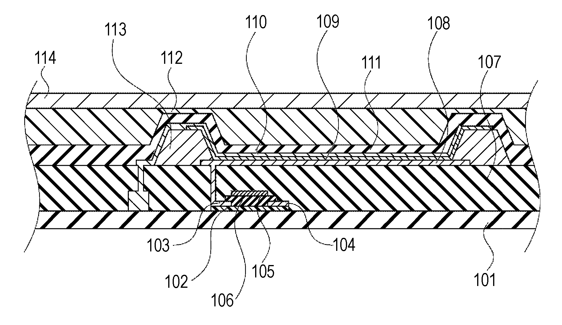
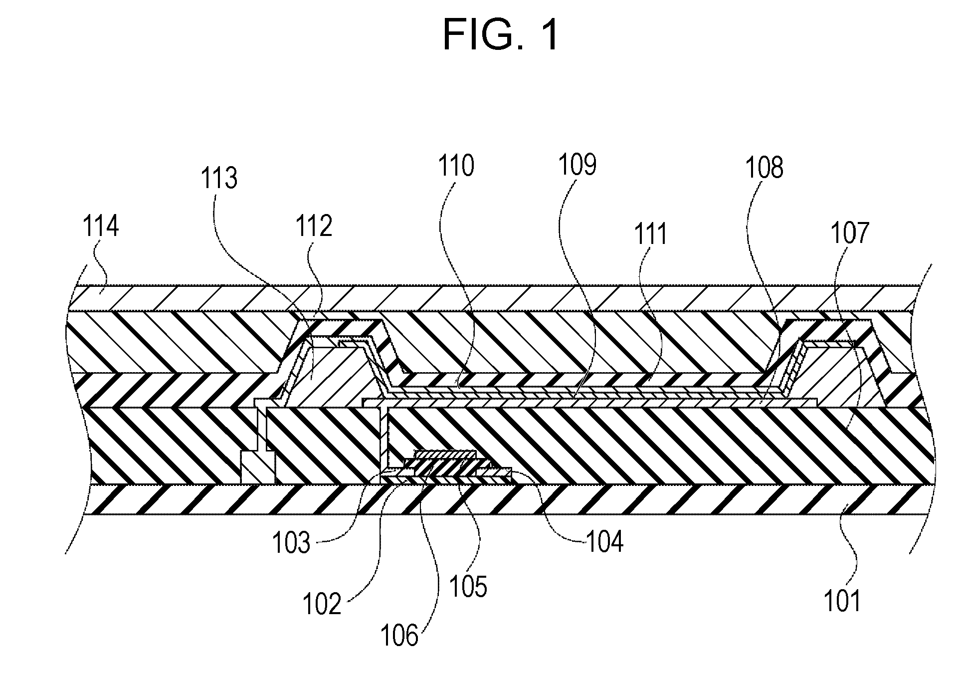
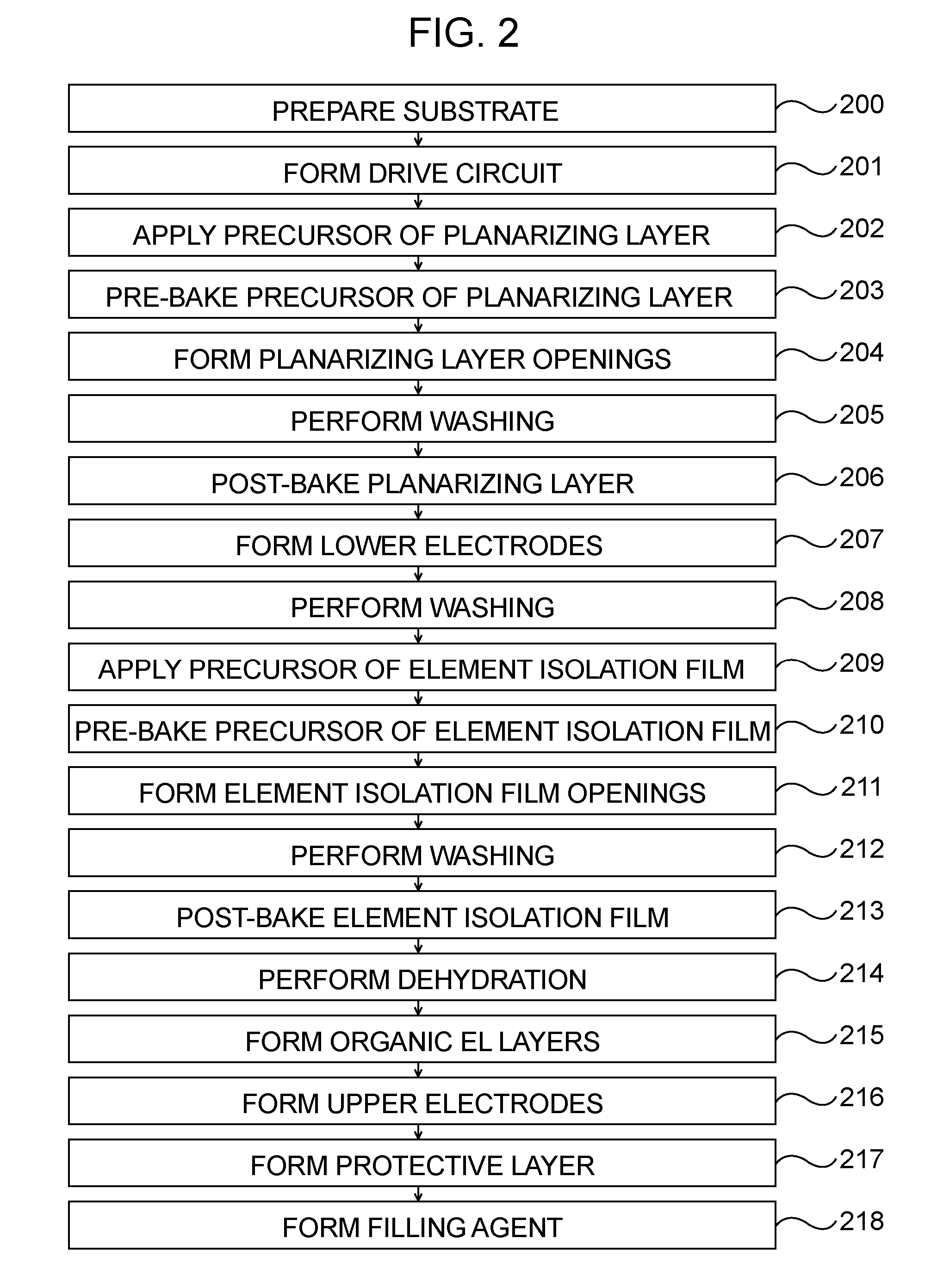
[0111] The organic EL elements shown in FIG. 1 were formed on a glass substrate 0.8 mm thick, 450 mm wide, and 550 mm long. On the glass substrate, a circuit shown in FIG. 3 was formed for each element using a low-temperature polycrystalline silicon thin film, which was recrystallized by a KrF excimer laser (wavelength of 248 nm). As a circuit protective layer, an insulating silicon nitride layer having a thickness of approximately 400 nm was deposited on the circuits by a plasma CVD method at a frequency of 13.56 MHz using a gas mixture containing a silane gas, an ammonium gas, and a hydrogen gas at a ratio of 1:1:10 as a starting material gas. A composition was prepared composed of 60% of an oligomer formed from 3% of methyl methacrylic acid and 97% of methylmethacrylate and 40% of an oligomer formed from 3% of methyl methacrylic acid and 97% of butylmethacrylate.

[0112] Subsequently, 25 parts by weight of this composition was added to 100 parts by weight of diethylene glycol meth...

example 2

[0127] An organic EL element panel was formed using a methacrylate oligomer having a molecular weight of 1,000, which was the oligomer used in Example 1, in a manner equivalent to that in Example 1, except that the temperature increasing rate was changed as shown in Table 3. The hardness of the planarizing layer and the amount of the remaining oligomer were measured in a manner equivalent to that in Example 1. When the temperature increasing rate was high, a non-reaction component evaporated. As a result, a desired hardness could not be obtained. In addition, the amount of the remaining oligomer was large. On the other hand, when the temperature increasing rate was low, the amount of the oligomer decomposed by heat increased. As a result, the distortion and the number of pin holes increased. To evaluate the reliability, the heat cycle between 100° C. to −20° C. was repeatedly performed 20 times while the organic EL element was turned on. Subsequently, the reliability was evaluated b...

example 3

[0129] A planarizing layer having a thickness of 2 μm was deposited on a glass substrate under the same conditions as those in Example 2, in which the planarizing layer was formed at a temperature increasing rate of 10° C. / minute. Cr equivalent to that forming the lower electrode was deposited on the planarizing layer by vacuum evaporation so as to have a thickness of 100 nm. Before the deposition of the Cr, the surface of the planarizing layer was left in the atmosphere for one day and was then further irradiated with UV rays right before the deposition. The surface treatment of the planarizing layer was performed by changing the time for UV irradiation. The contact angle of the planarizing layer was measured by using a measurement device sold under the trade name “Drop Master 700” manufactured by Kyowa Interface Science Co., Ltd. The results are shown in Table 4. The adhesion of Cr deposited on the surface of the planarizing layer having the contact angle as described above was ev...


PUM


Abstract

The present invention provides an organic EL display device having a planarizing layer, which is prevented from being distorted. The above organic EL display device has a planarizing layer, which retains 5% or less the oligomer used to form this layer.

Description

BACKGROUND OF THE INVENTION [0001] 1. Field of the Invention [0002] The present invention is related to an organic electroluminescent display device and a manufacturing method thereof, as well as the display device having a planarizing layer between switching elements and lower electrodes. [0003] 2. Description of the Related Art [0004] In recent years, organic electroluminescent elements (hereinafter referred to as “organic EL elements”) have been actively developed. [0005] Japanese Patent Laid-Open No. 10-189252 discloses an organic active EL light-emitting device in which thin-film transistors, an interlayer insulating film, and organic EL elements are provided. [0006] A layer provided between switching elements, such as thin-film transistors and lower electrodes of organic electroluminescent elements, is also called a planarizing layer. The planarizing layer covers the switching elements. [0007] Various phenomena occur when this planarizing layer is distorted. [0008] For example...

Claims


Application Information

Patent Timeline
Patent Type & Authority Applications(United States)
IPC IPC(8): H05B33/00
CPCH01L27/1248H01L27/3244H10K59/12
Inventor SAITO, KEISHI
Owner CANON KK
Why Eureka
Try Eureka