Wafer bonded epitaxial templates for silicon heterostructures

Inactive Publication Date: 2005-02-03
CALIFORNIA INST OF TECH
View PDF47 Cites 82 Cited by
  • Summary
  • Abstract
  • Description
  • Claims
  • Application Information

AI Technical Summary

Benefits of technology

The invention is an improvement in a method of epitaxially growing heterostructures on a virtual substrate comprised of an optoelectronic device substrate and handle substrate. The method comprises the step of initiating bonding of the device substrate to the handle substrate. The device substrate is composed of a material suitable for fabrication of optoelectronic devices therein and the handle substrate is composed of an inexpensive material suitable for providing mechanical sup

Problems solved by technology

However, these are prohibitively expensive for all but space applicati

Method used


Image

  • Wafer bonded epitaxial templates for silicon heterostructures
  • Wafer bonded epitaxial templates for silicon heterostructures
  • Wafer bonded epitaxial templates for silicon heterostructures

Examples


Embodiment Construction

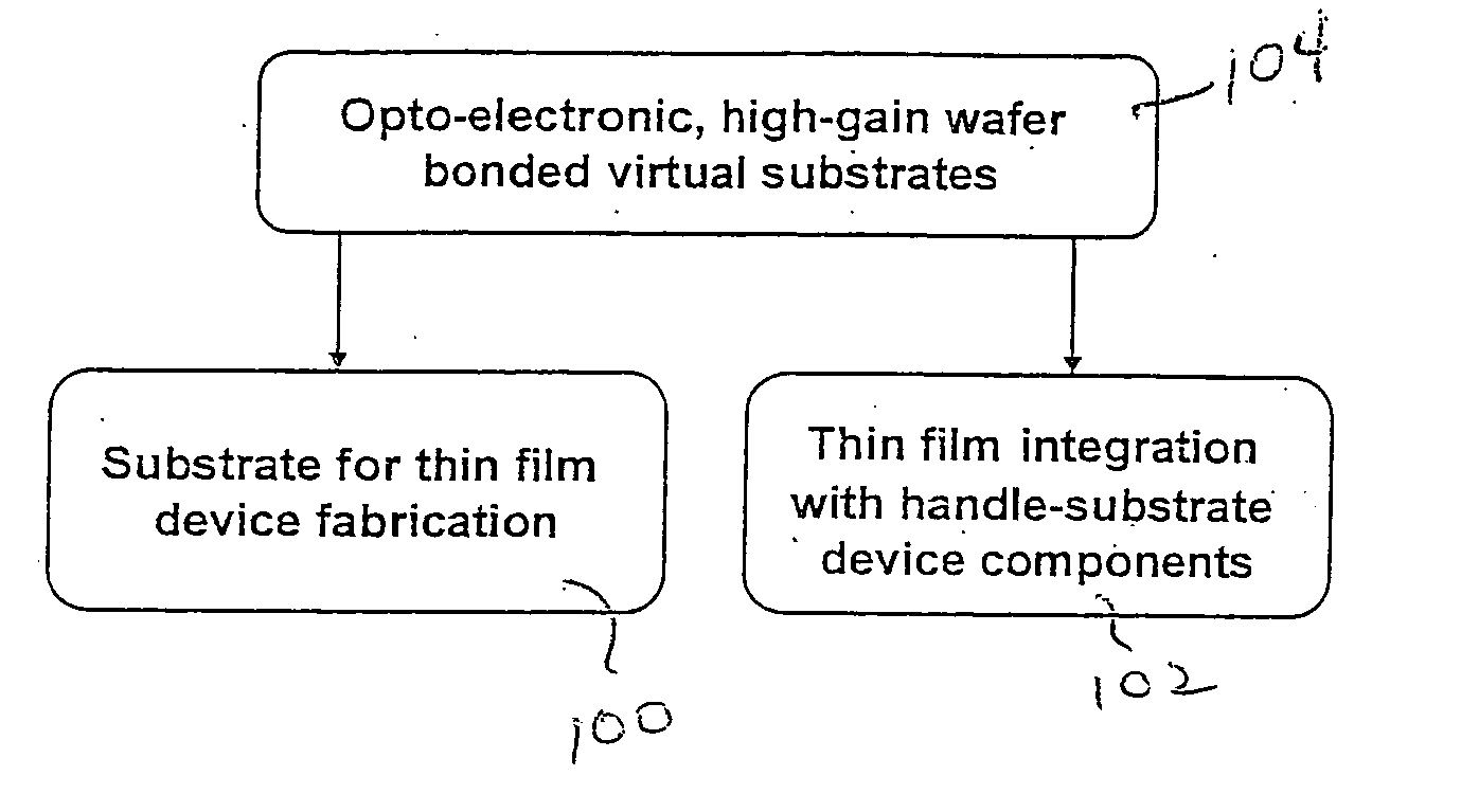
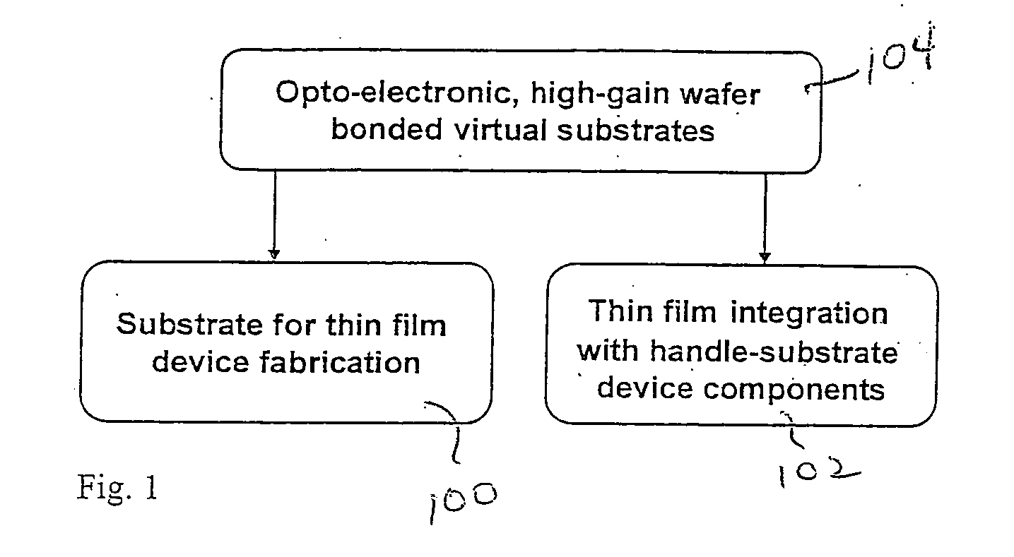
The fabrication 104 of virtual wafer bonded substrates could take two possible approaches as diagrammatically illustrated in the block diagram of FIG. 1. These approaches are the integration of a thin device film with a bulk substrate prior to fabricating a functional device indicated by block 100, or the device film can be transferred to the handle substrate following the fabrication of a functional logic device in the handle substrate and / or the fabrication of a functional optoelectronic device in the optoelectronic device substrate as depicted by block 102.

This specification summarizes a number of embodiments of the fabrication of optoelectronic virtual substrates. We begin with a summary of the technology generally employed and device structures for which the virtual substrate product can be used. Next, more material process steps are described in the order that they appear in the fabrication process.

Process And Product Overview

For the purpose of the specification the ter...


PUM


Abstract

A heterostructure device layer is epitaxially grown on a virtual substrate, such as an InP/InGaAs/InP double heterostructure. A device substrate and a handle substrate form the virtual substrate. The device substrate is bonded to the handle substrate and is composed of a material suitable for fabrication of optoelectronic devices. The handle substrate is composed of a material suitable for providing mechanical support. The mechanical strength of the device and handle substrates is improved and the device substrate is thinned to leave a single-crystal film on the virtual substrate such as by exfoliation of a device film from the device substrate. An upper portion of the device film exfoliated from the device substrate is removed to provide a smoother and less defect prone surface for an optoelectronic device. A heterostructure is epitaxially grown on the smoothed surface in which an optoelectronic device may be fabricated.

Description

BACKGROUND OF THE INVENTION 1. Field of the Invention The invention relates to the field of semiconductor processing of films and in particular to processing nonsilicon films on heterostructures. 2. Description of the Prior Art The optoelectronics, photovoltaics, telecommunications, and LED industries have a need for a substrate technology that allows them to use a low-cost readily available substrate like Si as a mechanical support for a thin film of optoelectronic material on which to fabricate a device. Some obvious advantages are improved mechanical strength and superior thermal conductivity relative to a bulk optoelectronic material. Group III-V semiconductor layered structures grown on bulk germanium substrates have been used in the prior art to create high efficiency triple-junction solar cells with efficiencies greater than 30%. However, these are prohibitively expensive for all but space applications, because the Ge substrate constitutes a large portion of this cost. ...

Claims


Application Information

Patent Timeline
IPC IPC(8): H01L21/302H01L21/461H01L31/0328H01L31/0336H01L31/072H01L31/109
CPCH01L21/187H01L21/30604H01L21/30612H01L21/30625Y02E10/50H01L31/0392H01L31/18H01L33/005H01L21/76254
Inventor ATWATER, HARRY A. JR.ZAHLER, JAMES M.MORRAL, ANNA FONTCUBERTAI
Owner CALIFORNIA INST OF TECH
Why Eureka
Try Eureka