Semiconductor device

a semiconductor and semiconductor technology, applied in the field of semiconductor devices, can solve the problems of increasing manufacturing costs, increasing manufacturing costs, and affecting the quality of semiconductor chips, and achieve the effects of high value-added portable electronic, not easily broken, and excellent portability

Inactive Publication Date: 2005-10-27
NEC CORP
View PDF12 Cites 174 Cited by
  • Summary
  • Abstract
  • Description
  • Claims
  • Application Information

AI Technical Summary

Benefits of technology

[0010] Accordingly, it is an object of the present invention to provide a low-cost semiconductor device which has various functions and facilitates mixed mounting of a plurality integrated circuits.
[0012] It is a further object of the present invention to provide a semiconductor device which achieves an excellent heat discharging characteristic by using a flexible substrate having a high thermal conductivity.
[0015] According to the present invention, an integrated circuit is formed on the top surface of a flexible substrate, and a plurality of flexible integrated circuit boards are mounted as a system on a separate support substrate, thereby achieving a low-cost system integrated circuit device which is light and is not easily breakable. Modules with various functions, such as a memory card and a display, can be constructed by combining ICs having various functions. Furthermore, the semiconductor device of the invention can be used as a systematized integrated circuit part at a stage prior to a module stage.
[0016] The use of the present invention can realize a high value-added portable electronic device excellent in portability, such as light and high mechanical strength, and a component of such an electronic device.

Problems solved by technology

Conventional IC chips or semiconductor chips formed on a silicon wafer are not flexible themselves and are relatively vulnerable.
The yield at the step of separating a semiconductor IC chip from a silicon wafer and the step of transferring the semiconductor IC chip to the flexible resin sheet, thus increasing the manufacturing cost.
Therefore, the process becomes a single wafer process and thus takes a longer time.
As an IC chip is opaque and has a thickness of several micrometers or so, the range of application is limited.
However, the prior art techniques have the following problems.
S62-160292 has a problem such that an integrated circuit should be formed directly on the top surface of the IC card.
This requires an exclusive circuit design and process for each purpose of IC cards, leading to an increased manufacturing cost.
H7-202147 suffers an insufficient flexibility and an difficulty in adaptation to the purpose of manufacturing a high-density semiconductor device by laminating a plurality of integrated circuit boards.
The liquid crystal display apparatuses described in Japanese Patent No. 2953023 and Japanese Patent No. 3033123 have a problem such that a strip drive circuit board is fragile and is likely to be broken when being mounted on the glass substrate.
In addition, the drive circuit board has a thickness of 0.5 to 1.0 mm, making it difficult to laminate a plurality of circuit boards at a high density.
Further, the glass substrate has a low thermal conductivity, so that the circuit characteristic is likely to be deteriorated by the self-heating of the drive circuit.

Method used


Image

  • Semiconductor device
  • Semiconductor device
  • Semiconductor device

Examples


first embodiment

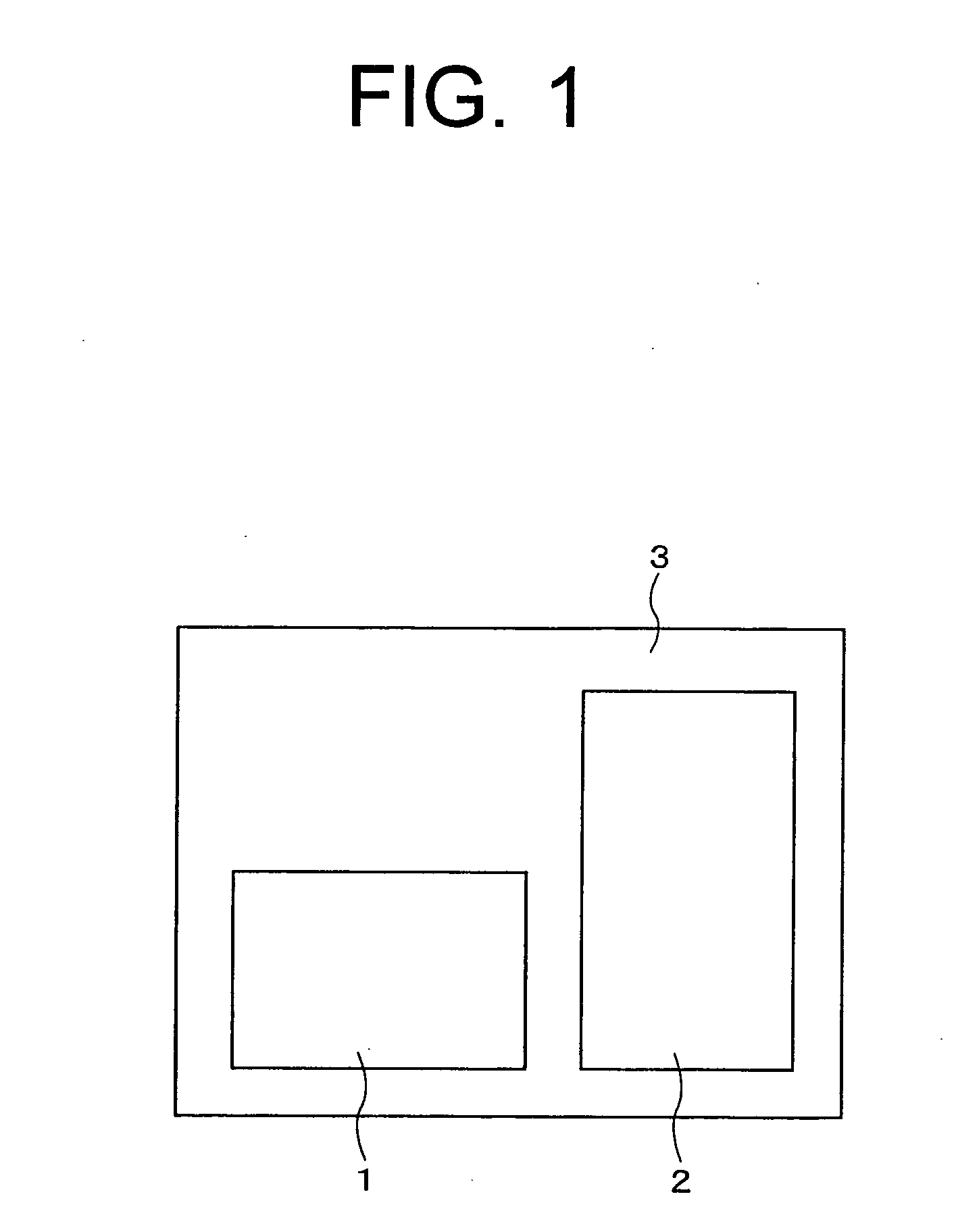
[0040] Preferred embodiments of the present invention will be described specifically below with reference to the accompanying drawings. To begin with, the present invention will be described. FIG. 1 is a plan view showing a semiconductor device according to the embodiment. As shown in FIG. 1, the semiconductor device of the embodiment is provided with a support substrate 3 on whose top surface flexible integrated circuit boards 1 and 2 are mounted. A plastic substrate, for example, is used for the support substrate 3. CMOS (Complementary Metal Oxide Semiconductor) integrated circuits formed by polycrystalline semiconductor TFTs (Thin Film Transistors) are formed on the top surfaces of the flexible integrated circuit boards 1 and 2

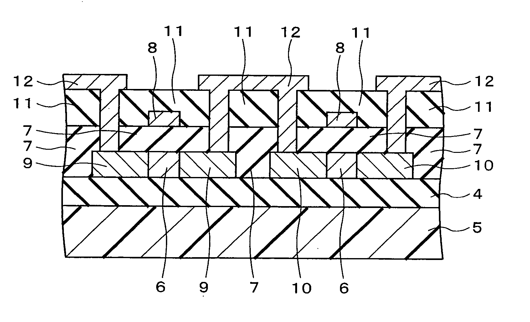
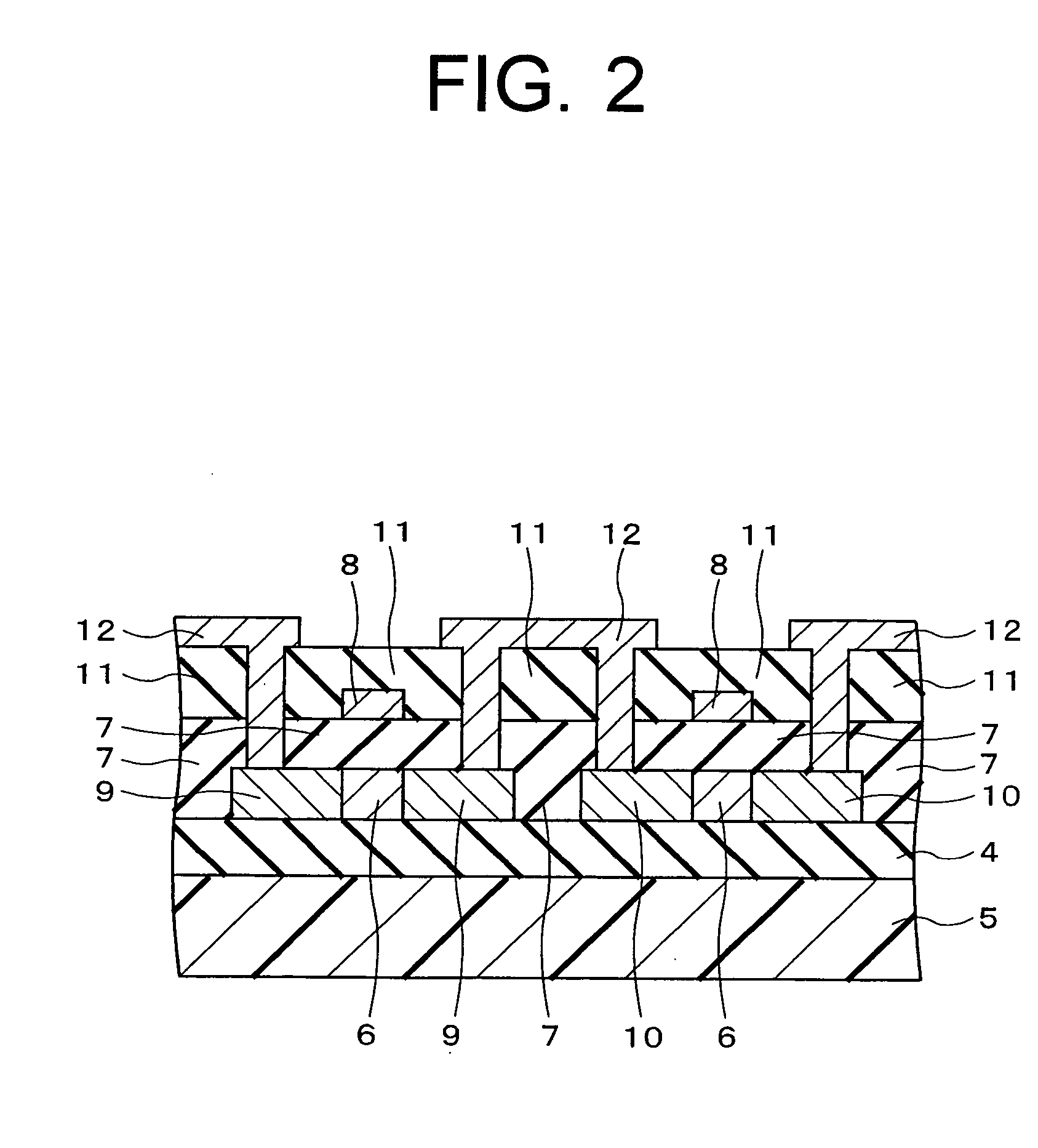
[0041]FIG. 2 is a cross-sectional view showing the basic structure of the CMOS circuit, and FIGS. 3A to 3F are cross-sectional views showing a manufacture method for the TFT step by step. As shown in FIG. 2, a TFT which is used in the semiconductor device o...

second embodiment

[0054]FIG. 8A is a plan view showing a second modification of the semiconductor device FIG. 8B is a cross-sectional view along line C-C in FIG. 8A, and FIG. 8C is a cross-sectional view along line D-D in FIG. 8A. As shown in FIGS. 8A and 8B, a glass substrate 29 is provided and a pixel circuit30 is formed on the top surface of the glass substrate 29 beforehand. The pixel circuit 30 is used in, for example, a display module, such as a liquid crystal display panel. The pixel circuit 30 has pixel electrodes (not shown) laid out in a matrix form, and a plurality of scan lines which transfer a scan pulse to the pixel electrodes and a plurality of data lines which transfer a video signal to the pixel electrodes are formed in such a way as to cross each other. An adhesive layer 24 is provided on the top surface of the glass substrate 29, and a flexible scan line drive circuit board 31 which outputs the scan pulse to the scan lines is mounted on the adhesive layer 24. The flexible scan lin...

third embodiment

[0059] In the semiconductor device with the above-described structure, as shown in FIG. 9, the flexible integrated circuit board 1 mounted on the support substrate 3 has a flexibility, so that if the flexible integrated circuit board 1 is mounted so as to extend from the top surface of the support substrate 3, a highly reliable semiconductor device can be realized.

[0060]FIG. 10 is a plan view showing a first modification of the semiconductor device according to the third embodiment. In the first modification of the third embodiment, as shown in FIG. 10, the flexible integrated circuit board 2 is further mounted on the flexible integrated circuit board 1 in the semiconductor device in FIG. 9.

[0061] According to the first modification of the semiconductor device according to the third embodiment with the above-described structure, when an integrated circuit board is further mounted on the semiconductor device of the third embodiment shown in FIG. 9, the flexible integrated circuit b...


PUM


Abstract

An integrated circuit is formed on a flexible substrate by using an amorphous semiconductor thin film, or a polycrystalline or a monocrystalline semiconductor thin film crystallized by laser annealing. A plurality of such flexible integrated circuit boards and mounted on a separate support substrate. This can enhance the mechanical strength of devices, such as an IC card and a liquid crystal display, and allow those devices to be manufactured at a low cost. It is also possible to provide a semiconductor device with a higher performance, on which a flexible integrated circuit board and an IC chip made from a silicon and / or glass wafer. Adhering a film substrate having a high thermal conductivity, such as a metal, to the bottom side of the flexible integrated circuit board improves the heat discharging characteristic of the integrated circuit and suppress the problem of self-heating.

Description

BACKGROUND OF THE INVENTION [0001] 1. Field of the Invention [0002] The present invention relates to a semiconductor device which has a plurality of integrated circuit boards mounted on a support substrate, and, more particularly, to a semiconductor device on which a plurality of flexible integrated circuit boards having different functions are mounted. [0003] 2. Description of the Related Art [0004] Recently, there is an increasing demand for IC cards incorporating a memory circuit or a microprocessor circuit as devices having a larger memory capacity than magnetic cards. Normally, this IC card is often carried around in a purse or the like, and is thus applied with bending force when being carried around. Conventional IC chips or semiconductor chips formed on a silicon wafer are not flexible themselves and are relatively vulnerable. The IC chips may therefore be broken by external force, like bending force, applied thereto. If such an IC chip is given a flexibility, it can be prev...

Claims


Application Information

Patent Timeline
Patent Type & Authority Applications(United States)
IPC IPC(8): G06K19/077H01L21/336H01L21/77H01L25/04H01L25/18H01L27/12H01L29/10H01L29/786
CPCH01L27/1214H01L24/18H01L29/78603H01L27/1266H01L27/1218H01L27/1274H01L2924/12042H01L2924/14H01L2924/00
Inventor TAKECHI, KAZUSHIGEKANOU, HIROSHI
Owner NEC CORP
Why Eureka
Try Eureka