These electronic devices have been traditionally fabricated using
silicon (Si) as a light-absorbing, semiconducting material in a relatively expensive production process.
A central challenge in cost-effectively constructing a large-area
copper-
indium-
gallium-di-
selenide (CIGS) based
solar cell or module is that the elements of the CIGS layer must be within a narrow stoichiometric ratio on nano-, meso-, and macroscopic
length scale in all three dimensions in order for the resulting
cell or module to be highly efficient.
Achieving precise
stoichiometric composition over relatively large substrate areas is, however, difficult using traditional vacuum-based deposition processes.
For example, it is difficult to deposit compounds and / or alloys containing more than one element by
sputtering or
evaporation.
Both techniques rely on deposition approaches that are limited to line-of-
sight and limited-area sources, tending to result in poor surface coverage.
Line-of-
sight trajectories and limited-area sources can result in non-uniform three-dimensional distribution of the elements in all three dimensions and / or poor film-thickness uniformity over large areas.
Such non-uniformity also alters the local stoichiometric ratios of the absorber layer, decreasing the potential power conversion efficiency of the complete
cell or module.
However, solar cells fabricated from the sintered
layers had very low efficiencies because the structural and electronic quality of these absorbers was poor.
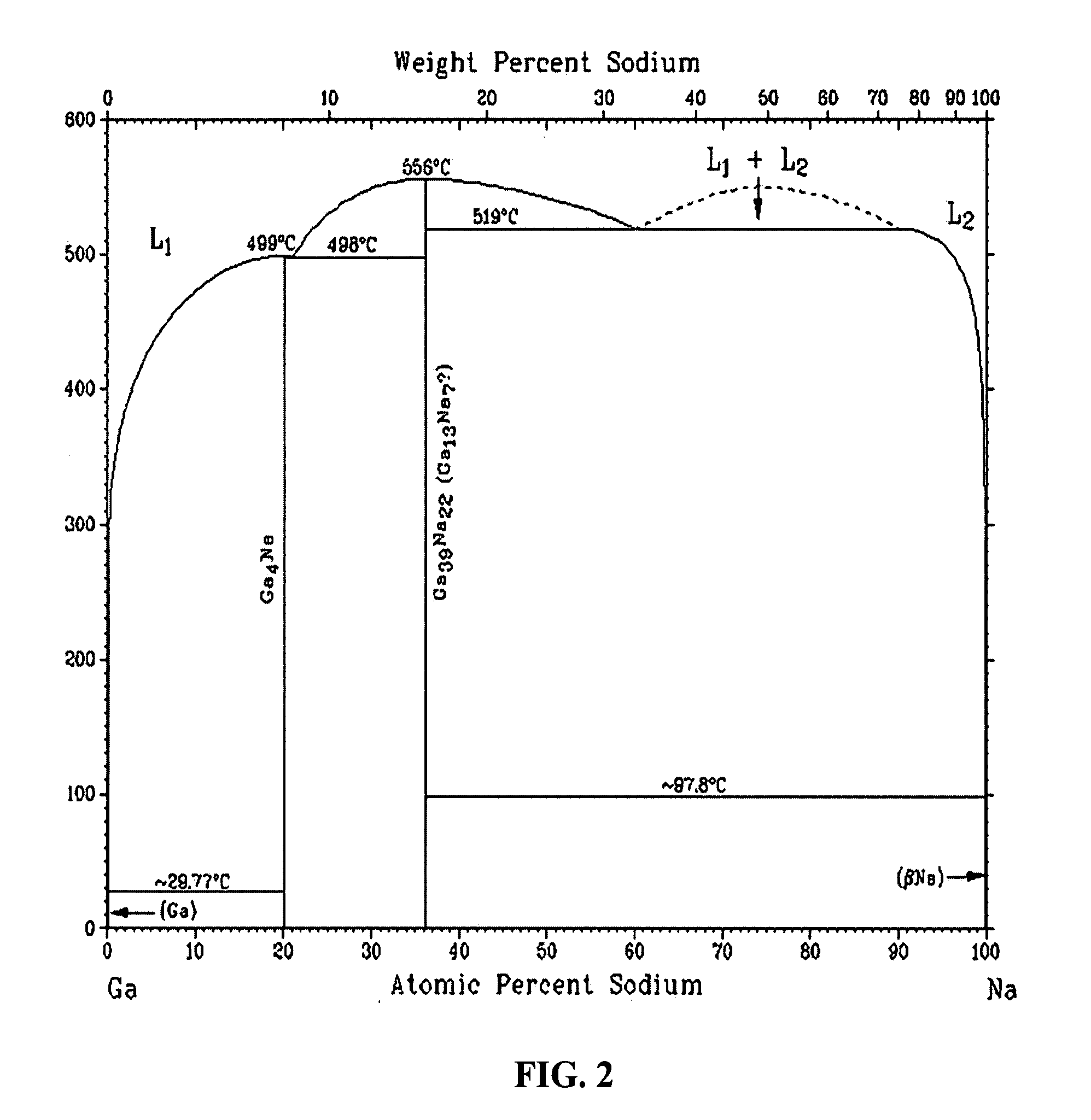
A difficulty in this approach was finding an appropriate fluxing agent for dense Cu—In—Se2 film formation.
These solvents and organic additives are typically unwanted in the final thin-film and require facile removal during or after the
deposition process.
Unfortunately, sometimes these preferably
solid components can become liquid at the handling and / or
particle size reduction temperatures typically associated with non-vacuum techniques for
solar cell production.
This may be a disadvantageous feature as premature and / or undesired liquification or coalescence increases the difficulty in handling these materials during
processing, during ink storage, and may require more involved techniques.
It may also be disadvantageous during
processing since the liquid form may change the
kinetics of the conversion of the particulate layer to the final
semiconductor film.
This can result in thickness non-uniformity and / or lateral composition non-uniformity.
For example for the preferably solid components, liquid form might be present and undesirable before / during the synthesis of the particles.
Such components in liquid form increases the difficulty in controlling and maintaining the particle (droplet) size during ink preparation and solution deposition.
Additionally, difficulty in controlling the particle (droplet) size during deposition complicates controlling and maintaining the target thickness uniformity of the resulting film on micro-, and macroscopic length scales.
Additionally for the preferably solid components, liquid might be present and undesirable when annealing the coatings of ink.
It may also be disadvantageous during single and / or multi-step conversion of the solution-deposited
coating or layer into the resulting semiconductor film since the premature presence of liquid may change the
kinetics of the reactions involved and therefore the quality and uniformity of the semiconductor film.
For example, if too much liquid is present at or near the onset of a reaction, liquid may dewet from the surface and ball up resulting in a non-uniform
material distribution throughout the layer, both in thickness and composition.

