

Thin film transistor including low resistance conductive thin films and manufacturing method thereof
- Summary
- Abstract
- Description
- Claims
- Application Information
AI Technical Summary
Benefits of technology
Problems solved by technology
Method used
Image

Examples
first embodiment
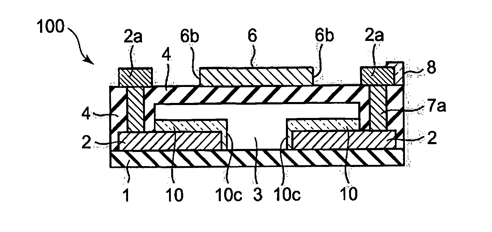
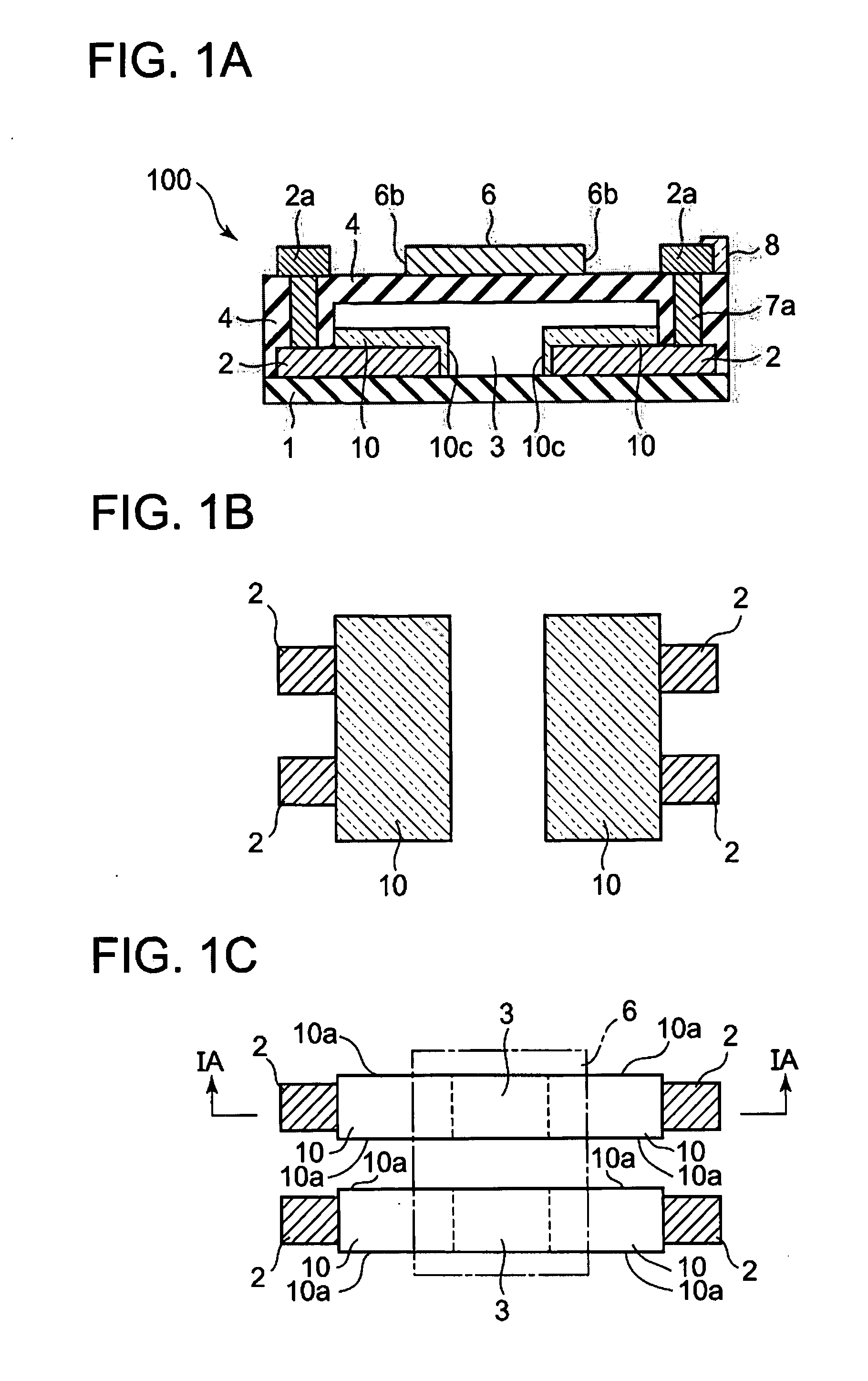
[0031] A thin film transistor 100 according to the present invention includes a substrate 1, a pair of source / drain electrodes 2, a pair of low resistance conductive thin films 10, an oxide semiconductor thin film layer 3, a gate insulating film 4, a gate electrode 6, contact parts 7a, a pair of external source / drain electrodes 2a, and a display electrode 8, which are laminated in the order shown in FIG. 1A.
[0032] The thin film transistor 100, as shown in FIG. 1A, is formed on a substrate 1 made of glass (non-alkali glass primarily comprising SiO2 and Al2O3). The material for the substrate 1 is not limited to glass, and other insulating materials, such as plastics covered with an insulator and metal foils covered with an insulator, are applicable to form the substrate 1 according to the present invention.
[0033] The pair of the source / drain electrodes 2 is laminated on the upper surface of the substrate 1. The source / drain electrodes 2 include a source electrode and a drain electrod...
second embodiment
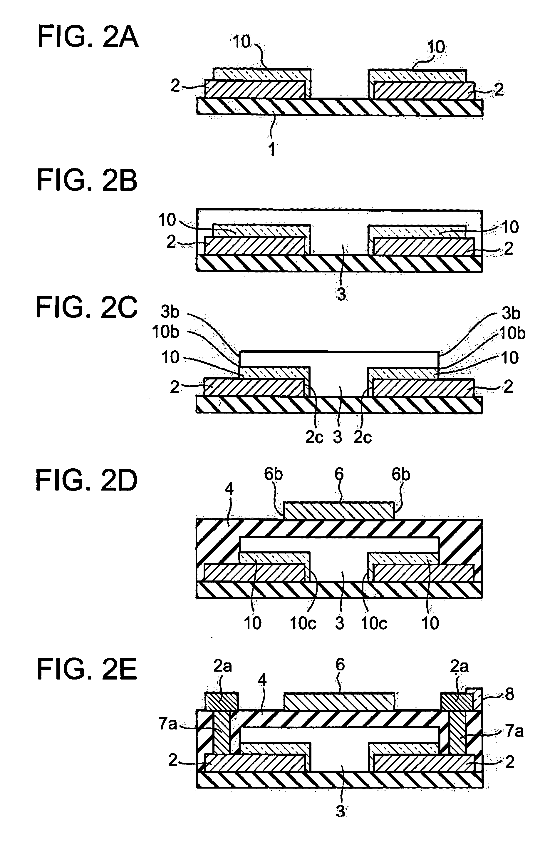
[0073] Hereinafter, a manufacturing method of a thin film transistor (TFT) according to the present invention will be explained referring to FIGS. 4A-4D.
[0074] First, as shown in FIG. 4A, source / drain electrodes 2 and low resistance conductive thin films 10 are formed on a substrate 1 as in the first embodiment of the present invention. The low resistance conductive thin films 10 are formed over the source / drain electrodes 2 of a plurality of TFTs 200. An oxide semiconductor thin film layer 3 is formed on all the exposed surfaces of the substrate 1, the source / drain electrodes 2, and the low resistance conductive thin films 10.
[0075] Next, as shown in FIG. 4B, a first gate insulating film 41 is formed on the oxide semiconductor thin film layer 3 using a technique and under a condition(s) that do not reduce the resistance of the oxide semiconductor thin film layer 3. Then, a photo-resist is coated on the first gate insulating film 41 and patterned. Using the patterned photo-resist a...
third embodiment
[0082] Hereinafter, the thin film transistor according to the present invention will be described with reference to FIG. 5.
[0083]FIG. 5 is a cross-sectional view showing the structure of a thin film transistor 300 according to the third embodiment of the present invention. The thin film transistor 300 includes a substrate 11, a gate electrode 12, a gate insulating film 13, source / drain electrodes 14, low resistance conductive thin films 20, an oxide semiconductor thin film layer 15, an overcoat insulating film 16, external source / drain electrodes 14a, contact parts 18a, and a display electrode 19. The TFT 300 is a bottom gate type TFT in which these layers are laminated in the order shown in FIG. 5.
[0084] As shown in FIG. 5, the thin film transistor 300 is formed on the substrate 11. The gate electrode 12 is formed on the substrate 11. In this step, the gate electrode 12 is disposed over the substrate 11 so that the outer ends of the gate electrode 12 will be positioned outside the...
PUM
 Abstract
Description
Claims
Application Information