Semiconductor device and manufacturing method thereof

a technology of semiconductors and semiconductors, applied in the direction of radiation control devices, identification means, instruments, etc., can solve the problems of complex process and non-normal operation of display panels, and achieve the effect of low resistance of wires

Active Publication Date: 2007-05-17
SEMICON ENERGY LAB CO LTD
View PDF98 Cites 4301 Cited by
  • Summary
  • Abstract
  • Description
  • Claims
  • Application Information

AI Technical Summary

Benefits of technology

[0033] Since Al is used for a part of the source electrode and drain electrode, low resistance of a wire can be obtained.

Problems solved by technology

If the current value is high, a display panel does not operate normally.
However, a process becomes complex when the light shielding film is formed, because a deposition step, a photolithography step, and an etching step are required.

Method used


Image

  • Semiconductor device and manufacturing method thereof
  • Semiconductor device and manufacturing method thereof
  • Semiconductor device and manufacturing method thereof

Examples


embodiment 1

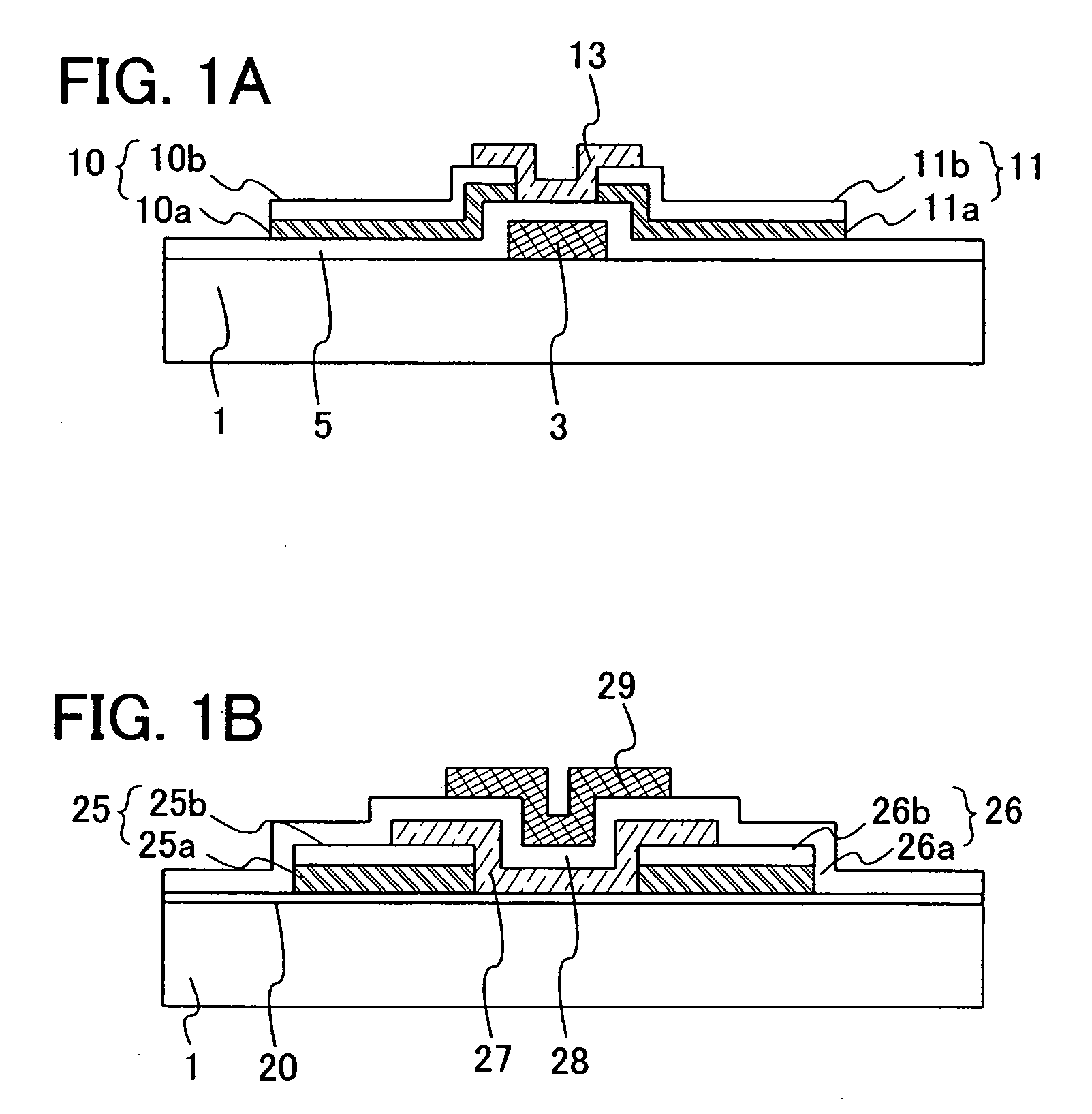
[0052] Here, a bottom gate semiconductor device is described.

[0053]FIG. 1A is a cross-sectional view in which one example of the embodiment of this invention is shown. In FIG. 1A, numeral reference 1 denotes a substrate, 3 denotes a gate electrode, 5 denotes a gate insulating film, 10 denotes a source electrode, 10a denotes a first conductive film, 10b denotes a second conductive film, 11 denotes a drain electrode, 11a denotes a first conductive film, 11b denotes a second conductive film, and 13 denotes a semiconductor film. An insulating film for passivation or planarization may be formed over the semiconductor film 13.

[0054] The gate electrode 3 is formed over the substrate 1, the gate insulating film 5 is formed over the gate electrode 3, and the source electrode 10 and the drain electrode 11 are formed over the gate insulating film 5. The source electrode 10 is formed of a layered film having the first conductive film 10a and the second conductive film 10b, and the drain elect...

embodiment 2

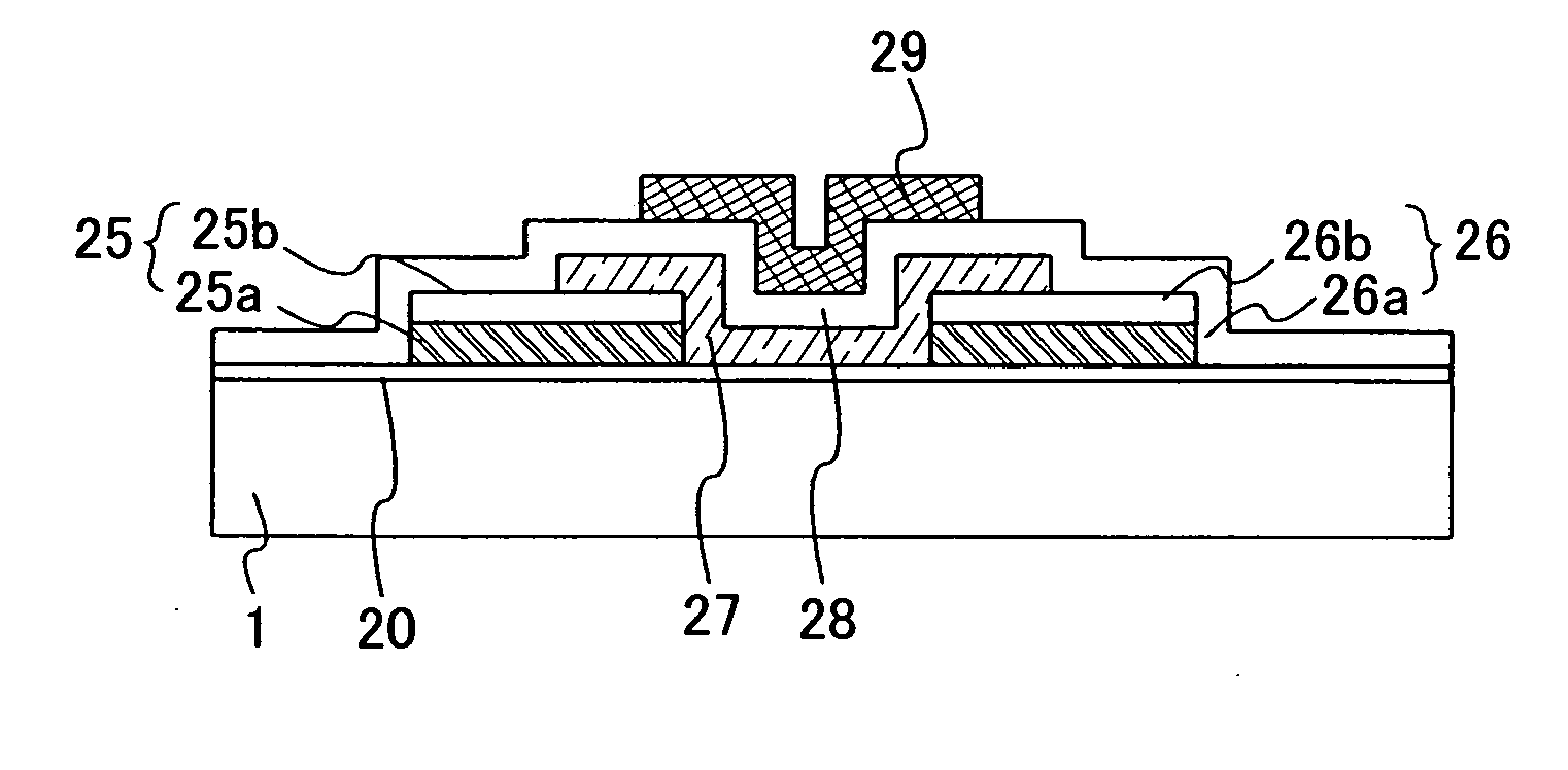
[0070] Here, a top gate semiconductor device is described.

[0071]FIG. 1B is a cross-sectional view showing one example of an embodiment of this invention. In FIG. 1B, numeral reference 1 denotes a substrate, 20 denotes an insulating film, 25 denotes a source electrode, 25a denotes a first conductive film, 25b denotes a second conductive film, 26 denotes a drain electrode, 26a denotes a first conductive film, 26b denotes a second conductive film, 27 denotes a semiconductor film, 28 denotes a gate insulating film, and 29 denotes a gate electrode. An insulating film for passivation or planarization may be formed over the gate electrode.

[0072] The insulating film 20 is formed on the substrate 1, and the source electrode 25 and the drain electrode 26 are formed over the insulating film 20. The source electrode 25 is formed with a layered film of the first conductive film 25a and the second conductive film 25b, and the drain electrode 26 is formed with a layered film of the first conduct...

embodiment 3

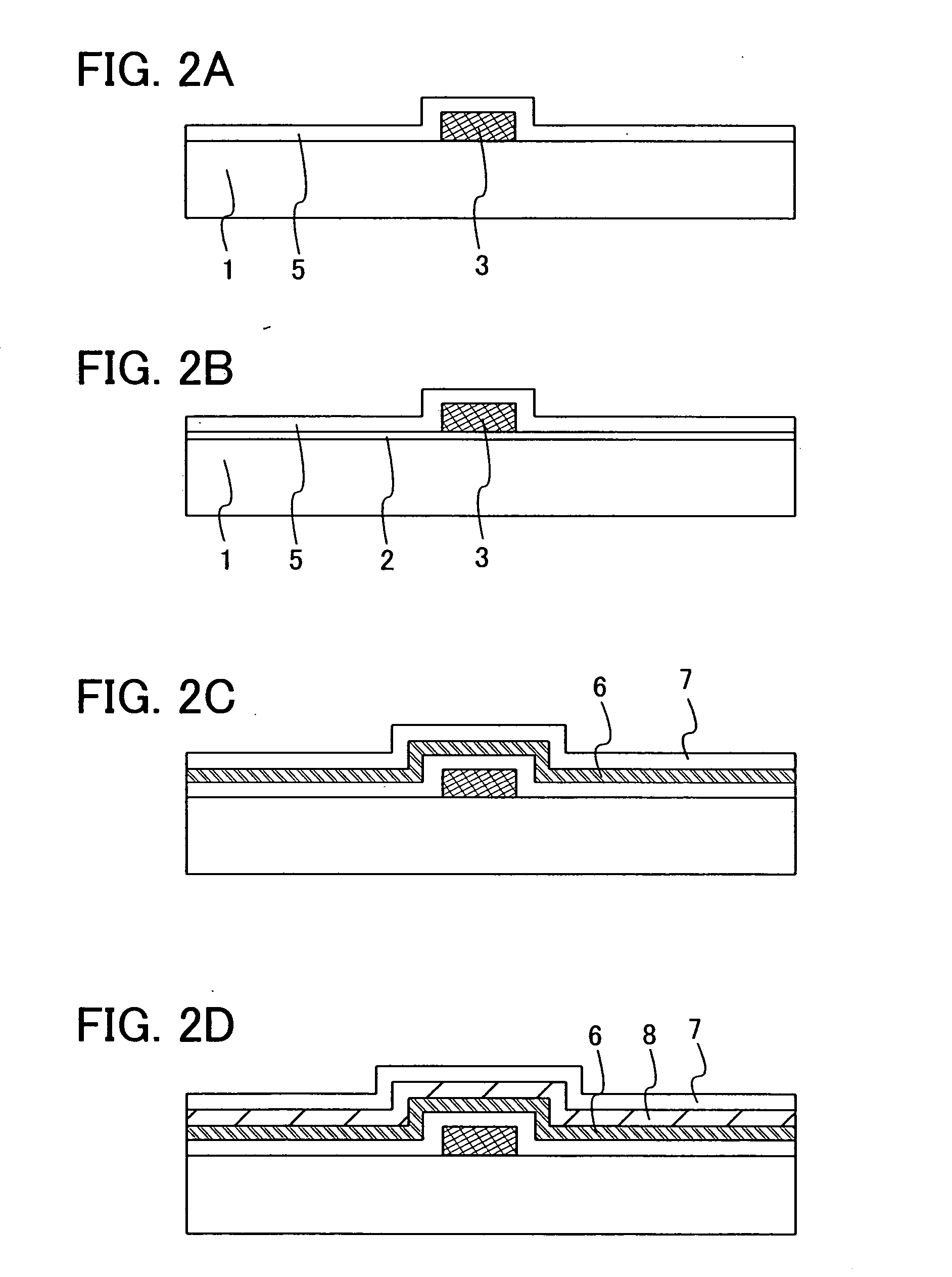
[0082] A manufacturing method of the bottom gate semiconductor device is described, in which a silicon oxide film or a silicon oxynitride film is formed as a gate insulating film over the gate electrode, an Al film or an Al alloy film is formed as a first conductive film, and a ZnO film to which an n-type or p-type impurity is added is formed as a second conductive film, and then, the second conductive film is etched to have an island-like shape by a first etching and the first conductive film is etched to have an island-like shape by a second etching to form source and drain electrodes, and a ZnO semiconductor film is formed.

[0083] As shown in FIG. 2A, a gate electrode 3 is formed. The thickness of the gate electrode may be 10 to 200 nm over a substrate 1. The substrate 1 may be formed by using the material shown in Embodiment 1. Here, a glass substrate is used.

[0084] An insulating film 2 containing silicon oxide (SiOx), silicon nitride (SiNx), silicon oxynitride (SiOxNy) (x>y), ...


PUM

PropertyMeasurementUnit
band gapaaaaaaaaaa
thicknessaaaaaaaaaa
temperatureaaaaaaaaaa

Abstract

To provide a semiconductor device in which a defect or fault is not generated and a manufacturing method thereof even if a ZnO semiconductor film is used and a ZnO film to which an n-type or p-type impurity is added is used for a source electrode and a drain electrode. The semiconductor device includes a gate insulating film formed by using a silicon oxide film or a silicon oxynitride film over a gate electrode, an Al film or an Al alloy film over the gate insulating film, a ZnO film to which an n-type or p-type impurity is added over the Al film or the Al alloy film, and a ZnO semiconductor film over the ZnO film to which an n-type or p-type impurity is added and the gate insulating film.

Description

TECHNICAL FIELD [0001] The present invention relates to a semiconductor device using ZnO (Zinc Oxide) and a manufacturing method thereof. BACKGROUND ART [0002] A semiconductor device used for a display panel of a liquid crystal display device or an EL (Electroluminescent) display device, for example, a semiconductor portion of a TFT (Thin Film Transistor), is generally formed by using a-Si (amorphous silicon) or poly-Si (polycrystalline silicon). [0003] Si (silicon) does not have a large band gap (for example, single-crystalline Si is 1.1 eV), and absorbs visible light. By irradiation with the light, electrons and holes (carriers) are formed in Si. If a Si film is used for a channel formation region of a TFT, a carrier is generated in the channel formation region by irradiation with the light even in an OFF state. Then, current flows between a source region and a drain region. The current which flows in an OFF state is called “OFF-leak current”. If the current value is high, a displ...

Claims


Application Information

Patent Timeline
Patent Type & Authority Applications(United States)
IPC IPC(8): H01L29/04G02F1/1333G02F1/1368G09F9/30H01L21/28H01L21/316H01L21/336H01L29/786H01L51/50H05B33/10H05B44/00
CPCH01L27/1214H01L29/41733H01L29/7869H01L29/4908H01L29/78621H01L29/45H01L27/1225H01L27/1255H01L21/02225H01L29/42312H01L29/4232H01L29/78696H01L21/02266
Inventor AKIMOTO, KENGO
Owner SEMICON ENERGY LAB CO LTD
Why Eureka
Try Eureka