Semiconductor integrated circuit apparatus with low wiring resistance

a technology of integrated circuit and low wiring resistance, which is applied in the direction of instruments, computer aided design, basic electric elements, etc., can solve the problems of deteriorating finishing precision of wiring, increasing manufacturing defective rate, and difficult to completely carry out flattening, so as to reduce the wiring resistance and improve the yield

Active Publication Date: 2011-09-20
PANASONIC SEMICON SOLUTIONS CO LTD
View PDF16 Cites 10 Cited by
  • Summary
  • Abstract
  • Description
  • Claims
  • Application Information

AI Technical Summary

Benefits of technology

[0034]In consideration of the actual circumstances, it is an object of the invention to provide a semiconductor integrated circuit which can easily be designed and has a low wiring resistance, and a method and apparatus for designing the semiconductor integrated circuit.

Problems solved by technology

As a first drawback, finishing precision in a wiring is deteriorated by a loading effect.
The loading effect is caused by an optical proximity effect in a photolithographic step and the excessive or insufficient amount of an etching gas in an etching step.
A second drawback relates to a controllability of an interlayer insulating film on a wiring layer.
For this reason, there is a problem in that a thickness of a film is reduced in a step portion or precision in the pattern is deteriorated to cause a disconnection, and a manufacturing defective rate is increased.
In the case in which a wiring pattern has a variation of density, however, it is hard to completely carry out the flattening.
A wiring in a microfabricating process has a problem to be considered in addition to the above drawbacks.
As a third drawback, a capacitance of the wiring is changed depending on the presence of an adjacent wiring.
As a result, the cross talk which causes noise and signal delay by coupling signal lines.
As a fourth drawback, a wiring resistance is increased.
Moreover, all of the flattened pattern generating methods according to the prior art serve to generate a redundant wiring which does not come in contact with a wiring in an empty region and only use the empty region for mainly generating a flattened pattern, and do not consider that a wiring resistance is reduced by using the empty region and there is a problem in that the wiring resistance is increased.
For this reason, a design becomes complicated.
In a designing method based on a minimum wiring width and wiring spacing as in a wiring grid used in an automatic place and route tool in an ASIC designing technique, particularly, there is a problem in that a design is complicated if a wide wiring is partially handled.

Method used


Image

  • Semiconductor integrated circuit apparatus with low wiring resistance
  • Semiconductor integrated circuit apparatus with low wiring resistance
  • Semiconductor integrated circuit apparatus with low wiring resistance

Examples


first embodiment

[0105]A first embodiment according to the invention will be described below in detail with reference to the drawings.

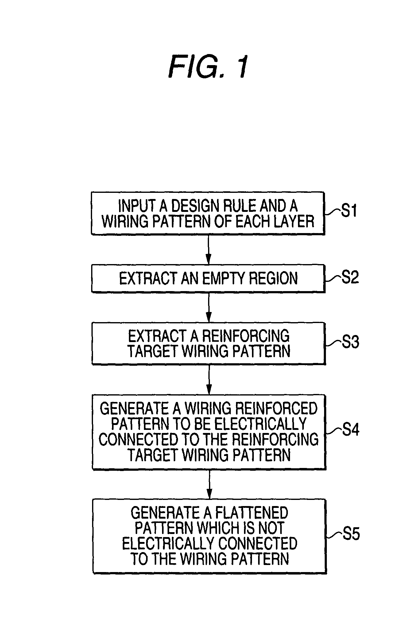
[0106]In the first embodiment, as shown in a flowchart of FIG. 1, an empty region having no wiring pattern is extracted (an empty region extracting step: S2) after an inputting step of inputting a design rule and a wiring pattern of each layer (S1), a reinforcing target wiring pattern for extracting a wiring pattern to be reinforced is extracted from the wiring pattern having an empty region provided around the wiring pattern by using the wiring pattern and information about the empty region (a reinforcing target wiring pattern extracting step: S3), a wiring reinforced pattern is generated and is electrically connected to the reinforcing target wiring pattern to obtain a uniform wiring pattern based on the design rule and an arrangement of the wiring pattern in the empty region provided around the reinforcing target wiring pattern (a wiring reinforced pattern generati...

second embodiment

[0118]A method of designing a wiring pattern of a semiconductor integrated circuit according to a second embodiment of the invention will be described below with reference to FIG. 4. Since a procedure for steps according to the second embodiment is the same as the processing procedure according to the first embodiment except for the wiring reinforced pattern generating step S4, description will be omitted.

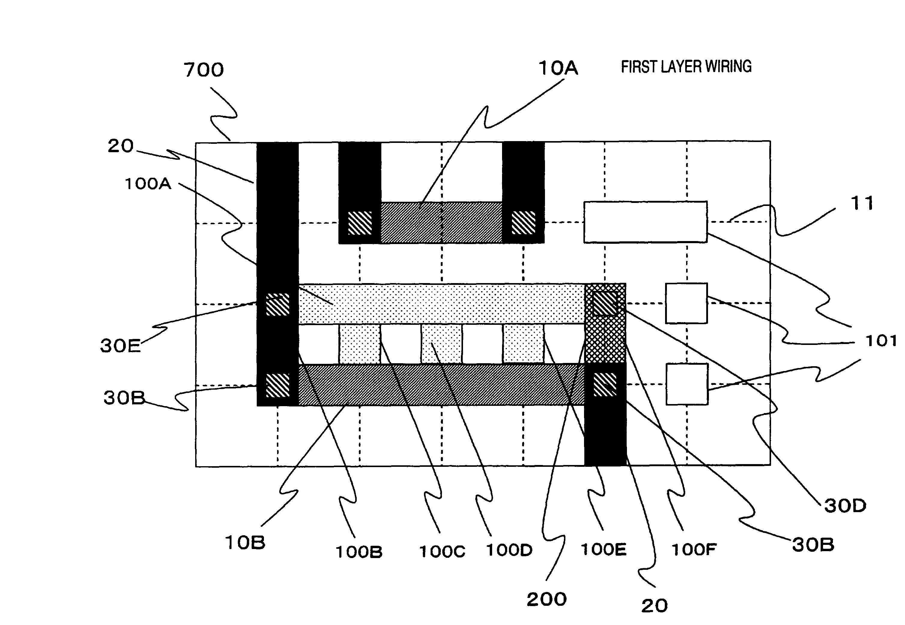
[0119]At the wiring reinforced pattern generating step S4, as shown in FIG. 4, a wiring reinforced pattern which takes a shape of a mesh and is to be electrically connected to the reinforcing target wiring pattern 10B is generated in accordance with the design rule in the empty region 12 provided around the reinforcing target wiring pattern 10B. More specifically, the wiring reinforced pattern 100 generates wiring reinforced patterns 100B, 100C, 100D, 100E and 100F in a perpendicular direction which are to be electrically connected to the reinforcing target wiring pattern 10B in ad...

third embodiment

[0123]Next, a method of designing a wiring pattern of a semiconductor integrated circuit according to a third embodiment of the invention will be described with reference to the drawings. FIG. 6 is a flowchart showing a processing procedure for a method of designing a layout of a semiconductor integrated circuit according to the third embodiment of the invention. An inputting step S1 is the same as that in the first embodiment. FIG. 24 shows a wiring pattern of each other which is to be input. FIG. 24 has been described in the Background Art.

[0124]Moreover, an empty region extracting step S2 to be a next step is the same as that in the first embodiment.

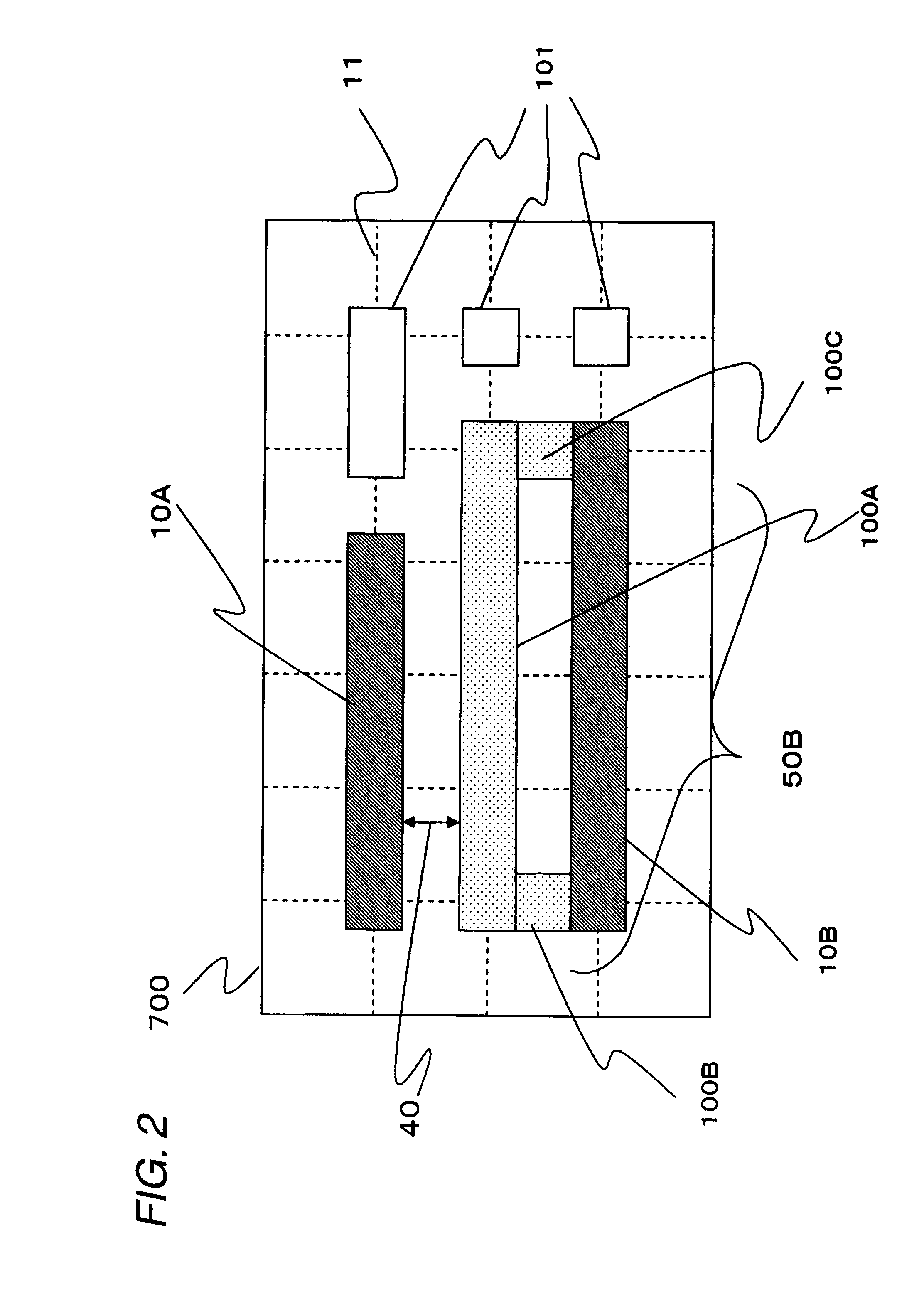
[0125]At a reinforcing target wiring pattern extracting step S31, then, the wiring pattern having an empty region on an upper layer or a lower layer of the wiring pattern is extracted as a wiring pattern to be reinforced by using the wiring pattern and the information about the empty region. In FIG. 7, wiring patterns 10A and 10B havi...


PUM


Abstract

It is an object to provide a semiconductor integrated circuit which can easily be designed and has a low wiring resistance, and a method and apparatus for designing the semiconductor integrated circuit.In a semiconductor integrated circuit apparatus according to the invention, a first wiring layer is provided with a plurality of signal wirings having an equal width which is disposed in parallel with each other at a regular interval, and at least two of the signal wirings which are adjacent to each other are electrically connected to each other.

Description

BACKGROUND OF THE INVENTION[0001]1. Field of the Invention[0002]The present invention relates to a semiconductor integrated circuit and a method and apparatus for designing a wiring pattern of the semiconductor integrated circuit, and more particularly to a semiconductor integrated circuit apparatus which is effective for designing a semiconductor integrated circuit using a multilayer wiring layer, a wiring pattern designing method and a wiring pattern designing apparatus.[0003]2. Description of the Related Art[0004]In a semiconductor integrated circuit apparatus, conventionally, a multilayer wiring technique has been used to enhance a degree of integration.[0005]If a wiring layer has the variation of wiring pattern density, there are the following two drawbacks.[0006]As a first drawback, finishing precision in a wiring is deteriorated by a loading effect. The loading effect implies a phenomenon in which a finishing dimension of the pattern fluctuates depending on the density of the...

Claims


Application Information

Patent Timeline
Patent Type & Authority Patents(United States)
IPC IPC(8): G06F17/50H01L27/118H01L23/58H01L23/48H01L23/52H01L29/40
CPCG06F17/5077H01L23/528H01L2924/0002H01L2924/00G06F30/394
Inventor SHINOMIYA, NORIKOMUKAI, KIYOHITO
Owner PANASONIC SEMICON SOLUTIONS CO LTD
Why Eureka
Try Eureka