

Transparent oxide semiconductor thin film transistors
a technology of transparent oxide and semiconductor thin film, applied in the direction of transistors, vacuum evaporation coatings, coatings, etc., can solve the problems of incompatibility of electronics based on si, even amorphous si, with temperature-sensitive plastic substrates, and the electronic properties of most organic semiconductors are generally inferior
- Summary
- Abstract
- Description
- Claims
- Application Information
AI Technical Summary
Problems solved by technology
Method used
Image

Examples
example i
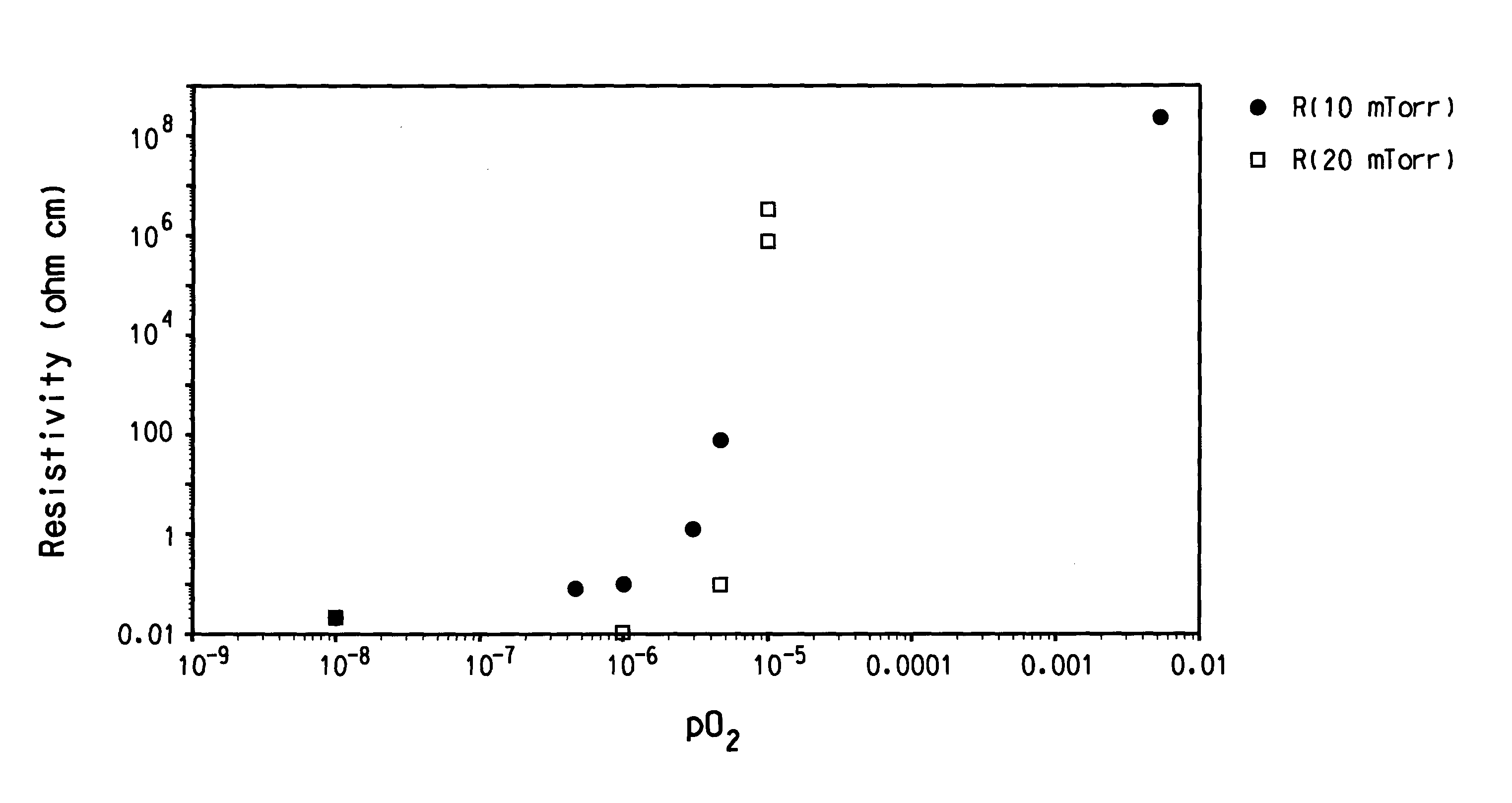
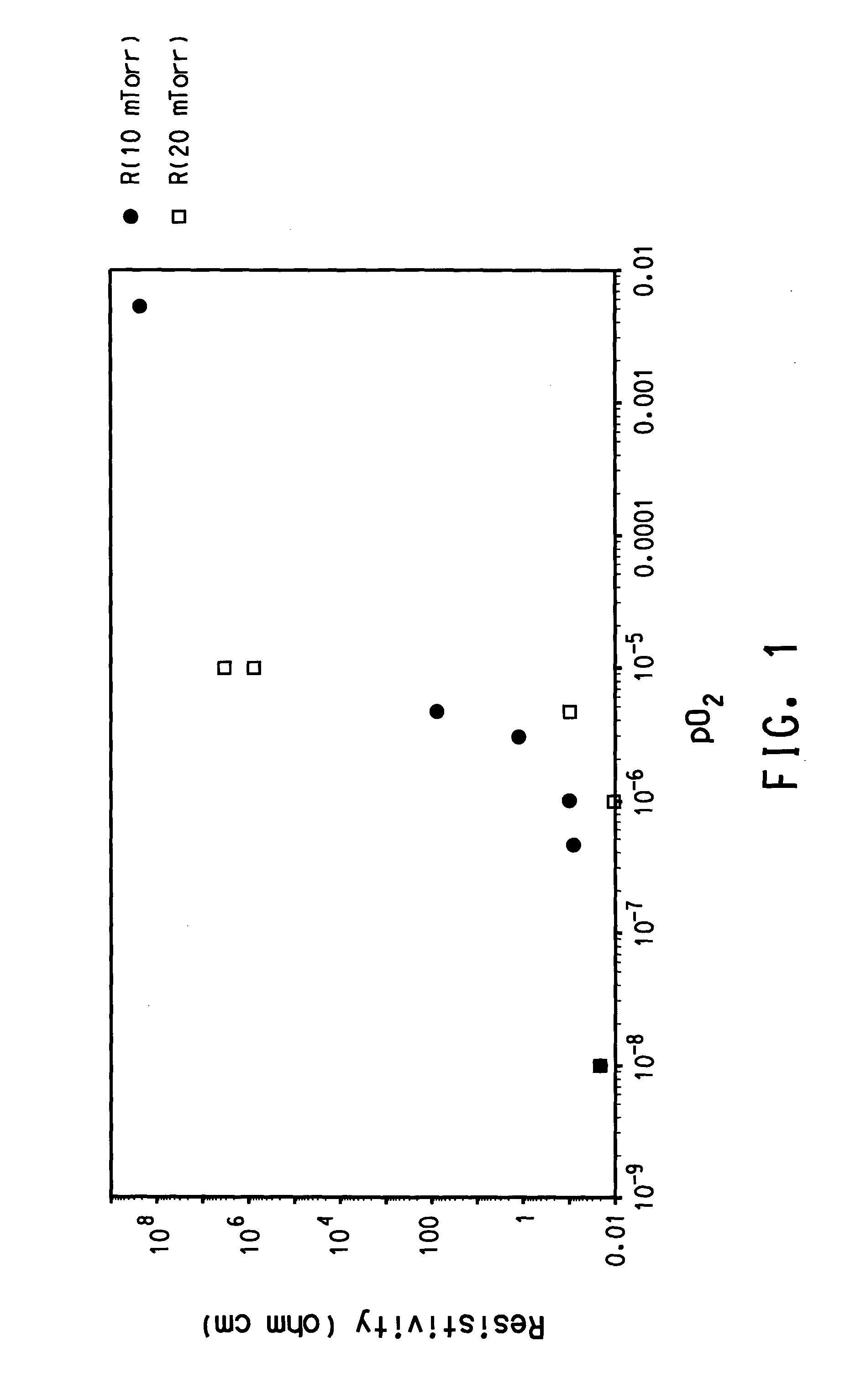
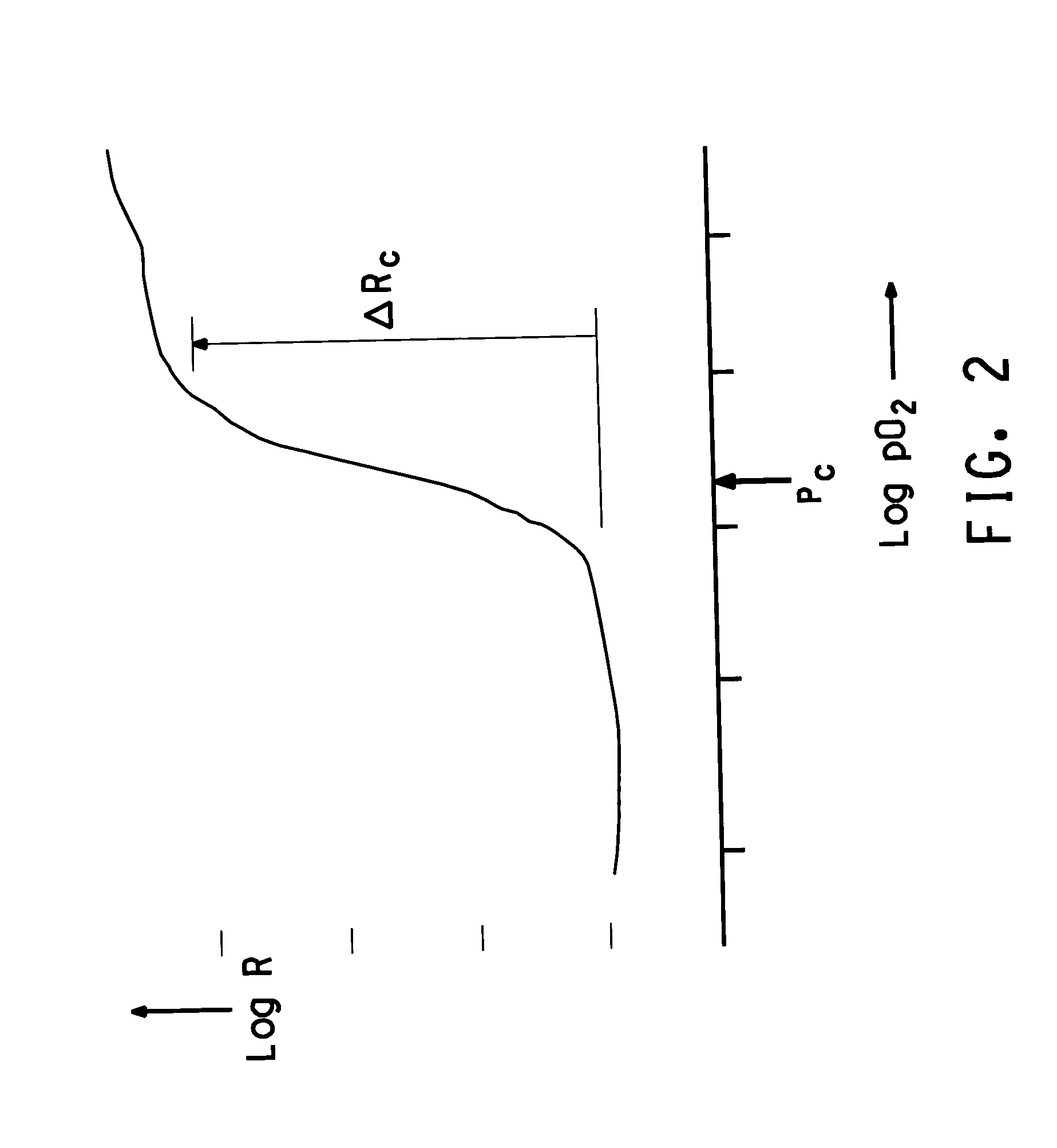
[0047] Using the transistor configuration shown in FIG. 3, a ZnO thin film semiconductor was rf magnetron sputtered at room temperature to deposit between source and drain electrodes, using a shadow mask. The ZnO target was 6.5 inch diameter and the rf power for sputtering was 100 W. The total gas pressure during sputtering was 20 mTorr, comprised of 1.times.10.sup.-5 Torr of oxygen, or pO.sub.2=P.sub.c, with the balance being argon. The ZnO film thickness, determined optically, was 849 A for a sputtering time of 500 sec. FIG. 4 is a set of corresponding drain current (I.sub.d) versus drain voltage (V.sub.d) transistor curves for gate voltages (V.sub.g) between zero and 50 V. For this device, the field effect mobility (.mu..sub.FE) from the linear current-voltage characteristics was determined to be 1.2 cm.sup.2 / V-s with an on / off ratio equal to 1.6.times.10.sup.6. This on / off ratio corresponds to the ratio of source-drain current with 50 V and 0 V bias on the gate electrode while a...
example 2
[0048] Using the transistor configuration shown in FIG. 3, a ZnO thin film semiconductor was rf magnetron sputtered at room temperature to deposit between source and drain electrodes, using a shadow mask. The ZnO target was 6.5 inch diameter and the rf power for sputtering was 100 W. The total gas pressure during sputtering was 20 mTorr, comprised of 2.times.10.sup.-5 Torr of oxygen, or pO.sub.2=2P.sub.c, with the balance being argon. The ZnO film thickness, determined optically, was 677 A for a sputtering time of 500 sec. FIG. 5 is a set of corresponding drain current (Id) versus drain voltage (Vd) transistor curves for gate voltages (Vg) between zero and 50 V. For this device, the field effect mobility (.mu..sub.FE) from the linear current-voltage characteristics was determined to be 0.3 cm.sup.2 / V-s with an on / off ratio equal to 1.0.times.10.sup.5.
example 3
[0049] Using the transistor configuration shown in FIG. 3, a ZnO thin film semiconductor was rf magnetron sputtered at room temperature to deposit between source and drain electrodes, using a shadow mask. The ZnO target was 6.5 inch diameter and the rf power for sputtering was 100 W. The total gas pressure during sputtering was 20 mTorr, comprised of 0.75.times.10.sup.-5 Torr of oxygen, or pO.sub.2=0.75 P.sub.c, with the balance being argon. The ZnO film thickness, determined optically, was 897 A for a sputtering time of 500 sec. FIG. 6 is a set of corresponding drain current (I.sub.d) versus drain voltage (V.sub.d) transistor curves for gate voltages (V.sub.g) between zero and 50 V. For this device, the field effect mobility (.mu..sub.FE) from the saturation current-voltage characteristics was determined to be 6.8 cm.sup.2 / V-s with an on / off ratio equal to 1.times.10.sup.3.
PUM
| Property | Measurement | Unit |
|---|---|---|
| gate voltage | aaaaa | aaaaa |
| gate voltage | aaaaa | aaaaa |
| gate voltages | aaaaa | aaaaa |
Abstract
Description
Claims
Application Information