Method for Forming Conformal Nitrided, Oxidized, or Carbonized Dielectric Film by Atomic Layer Deposition

a technology of atomic layer deposition and dielectric film, which is applied in the direction of plasma technique, metal material coating process, coating, etc., can solve the problems of significantly low achieve significant growth rate of film per cycle of ald, improve film quality in grooves, and avoid oxidation or nitride. or carbonization

Active Publication Date: 2015-05-28
ASM IP HLDG BV
View PDF5 Cites 393 Cited by
  • Summary
  • Abstract
  • Description
  • Claims
  • Application Information

AI Technical Summary

Benefits of technology

[0007]The present inventors conducted research on the process sequence dependency of the quality of film in grooves and discovered that by reacting a precursor multiple times in one cycle using a reactant, and by changing reactants and reacting a precursor multiple times in one cycle, the film quality in grooves can be improved. For example, wet etch rate of the film in grooves was improved from 5 times that of the film on a top surface to 1.2 times that of the film on a top surface. However, growth rate of the film per cycle of ALD became significantly low, which became a problem. In view of the above, in an embodiment of the present invention, a method for forming a film on a patterned surface of a substrate by atomic layer deposition (ALD) processing comprises: (i

Problems solved by technology

However, growth rate of the film per cycle of ALD

Method used


Image

  • Method for Forming Conformal Nitrided, Oxidized, or Carbonized Dielectric Film by Atomic Layer Deposition
  • Method for Forming Conformal Nitrided, Oxidized, or Carbonized Dielectric Film by Atomic Layer Deposition
  • Method for Forming Conformal Nitrided, Oxidized, or Carbonized Dielectric Film by Atomic Layer Deposition

Examples


examples

[0047]In the following examples where conditions and / or structures are not specified, the skilled artisan in the art can readily provide such conditions and / or structures, in view of the present disclosure, as a matter of routine experimentation.

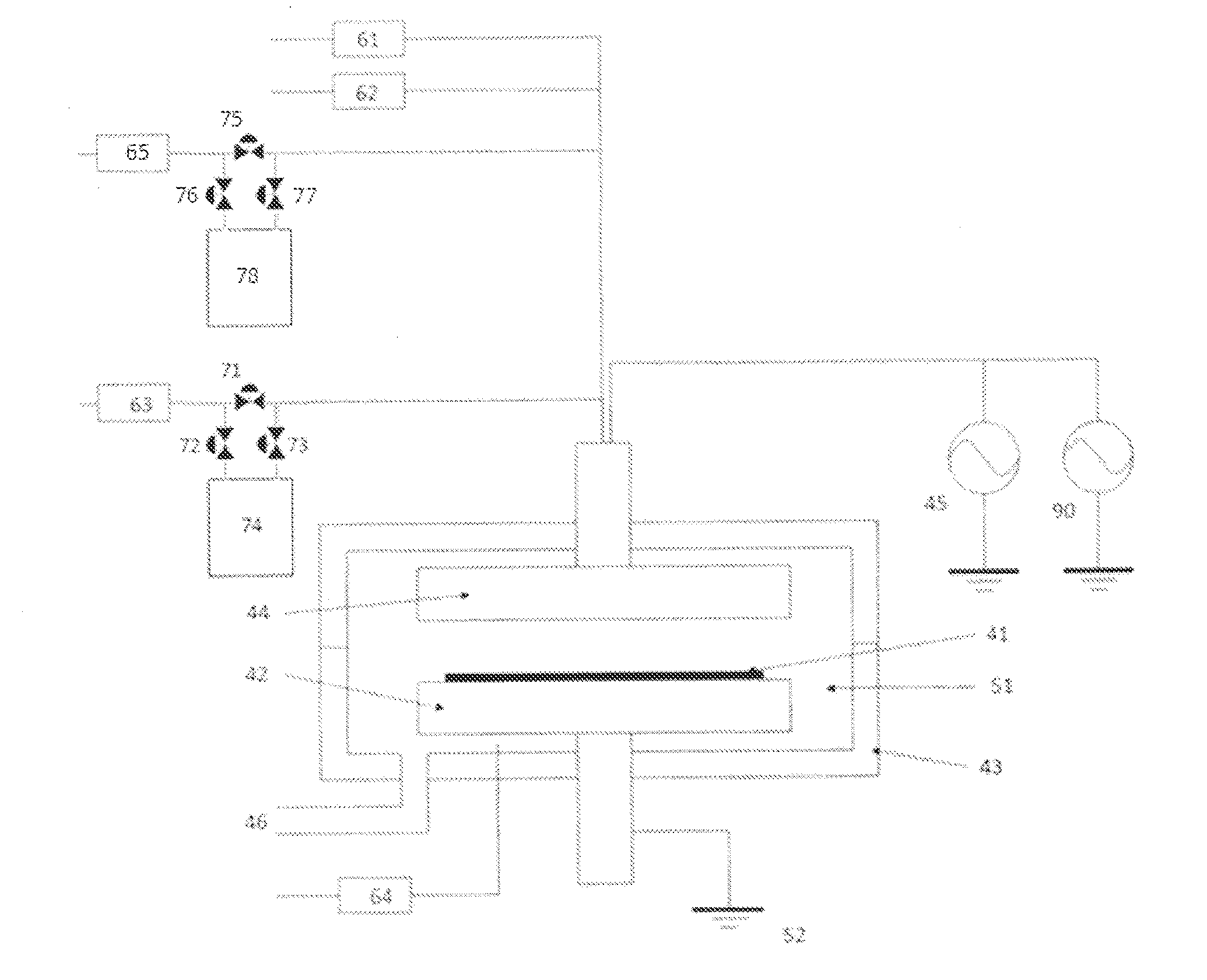
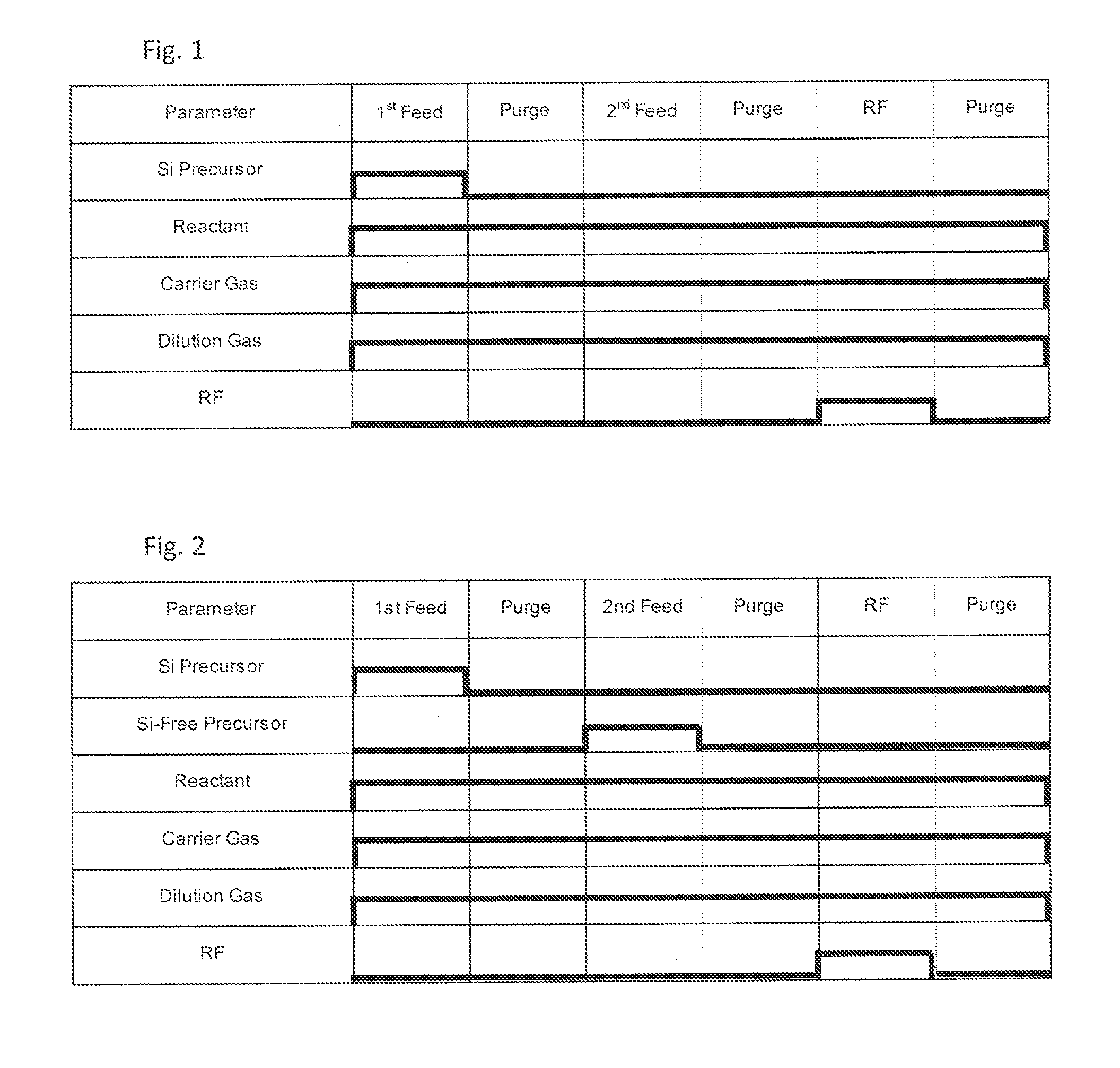
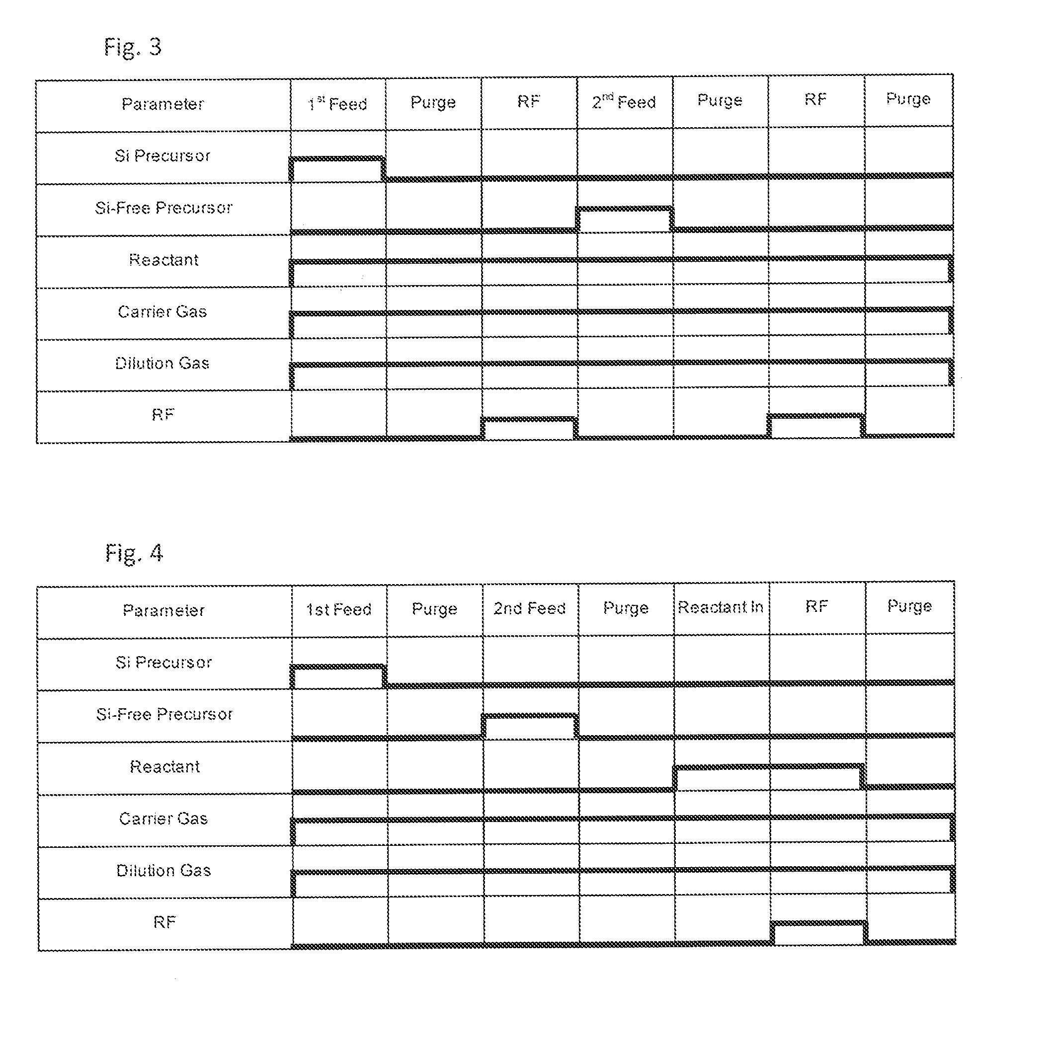
[0048]A dielectric film was deposited on a bare silicon substrate (Φ300 mm) by PEALD under common conditions shown in Table 2 below using the PEALD apparatus illustrated in FIG. 6. The specific conditions including the process sequence (SQ) are shown in Table 3. The flow rate of the precursor (g / cycle) was calculated based on the vapor pressure of the precursor and the temperature of the precursor in use. The SQ number corresponds to the figure number. The substrate had a flat surface and trenches having an opening width of about 40 nm and an aspect ratio of 1:7.5. The thickness of film was 350 nm for evaluating film properties.

TABLE 2Carrier gasAr; 2 SLMDilution gas100-2000 sccmSusceptor Temperature300° C.Distance between electrodes13 mmRF ...


PUM

PropertyMeasurementUnit
Temperatureaaaaaaaaaa
Weightaaaaaaaaaa
Dielectric polarization enthalpyaaaaaaaaaa

Abstract

A method for forming a film on a patterned surface of a substrate by atomic layer deposition (ALD) processing includes: adsorbing onto a patterned surface a first precursor containing silicon or metal in its molecule; adsorbing onto the first-precursor-adsorbed surface a second precursor containing no silicon or metal in its molecule; exposing the second-precursor-adsorbed surface to an excited reactant to oxidize, nitride, or carbonize the precursors adsorbed on the surface of the substrate; and repeating the above cycle to form a film on the patterned surface of the substrate.

Description

BACKGROUND OF THE INVENTION[0001]1. Field of the Invention[0002]The present invention generally relates to a method for forming a conformal nitrided, oxidized, or carbonized dielectric film by atomic layer deposition (ALD).[0003]2. Description of the Related Art[0004]As a method for depositing an insulation film on a substrate by ALD, substitution reaction by thermal reaction, plasma reaction, or remote plasma reaction is generally utilized. However, depending on the type of deposited film and the type of starting material, a problem may occur in that film quality is degraded because reaction in grooves of a recess pattern becomes insufficient, or secondary reaction such as physical adsorption interferes with reaction, or the like. In order to resolve the above problems, raising a process temperature and conducting post-process treatment are considered to be the most effective and have been widely conducted.[0005]The problems of the above solutions are that when a limitation is impo...

Claims


Application Information

Patent Timeline
IPC IPC(8): C23C16/34C23C16/452C23C16/56C23C16/40
CPCC23C16/345C23C16/401C23C16/56C23C16/452C23C16/403C23C16/4554
Inventor FUKAZAWA, ATSUKI
Owner ASM IP HLDG BV
Why Eureka
Try Eureka