Fused nanocrystal thin film semiconductor and method

a technology of nanocrystals and semiconductors, applied in the field of nanotechnology, can solve the problems of prohibitive equipment costs for providing high vacuum to process very large substrates, limiting the material choice and ultimate size of substrates,

Inactive Publication Date: 2008-04-10
HEWLETT PACKARD DEV CO LP
View PDF12 Cites 4036 Cited by
  • Summary
  • Abstract
  • Description
  • Claims
  • Application Information

AI Technical Summary

Problems solved by technology

The high temperatures as well as the requirements for achieving high vacuum during vacuum deposition often limit a material choice for and an ultimate size of a substrate.
For example, high temperatures can preclude the use of some plastics as a substrate material.
In addition, equipment costs for providing high vacuum to process very large substrates can be prohibitive.
However, while capable of being fabricated at relatively low temperatures (e.g., <150° C.) and using relatively lower cost manufacturing equipment, organic thin film semiconductors generally exhibit poor performance characteristics (e.g., very low carrier mobility) when compared to inorganic semiconductors.

Method used


Image

  • Fused nanocrystal thin film semiconductor and method
  • Fused nanocrystal thin film semiconductor and method
  • Fused nanocrystal thin film semiconductor and method

Examples


Embodiment Construction

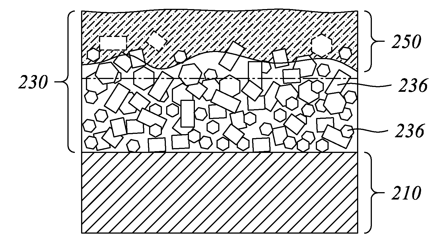
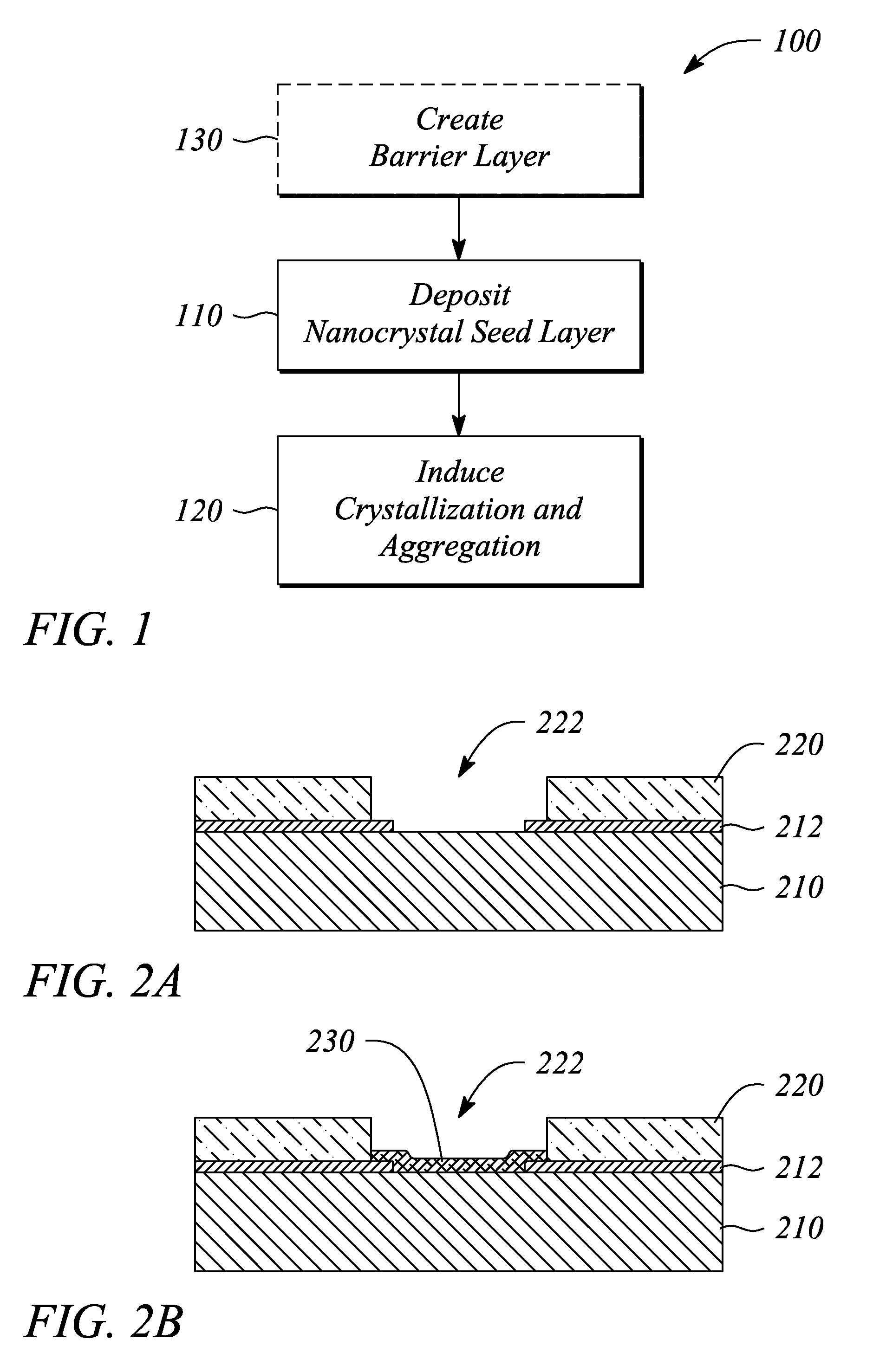
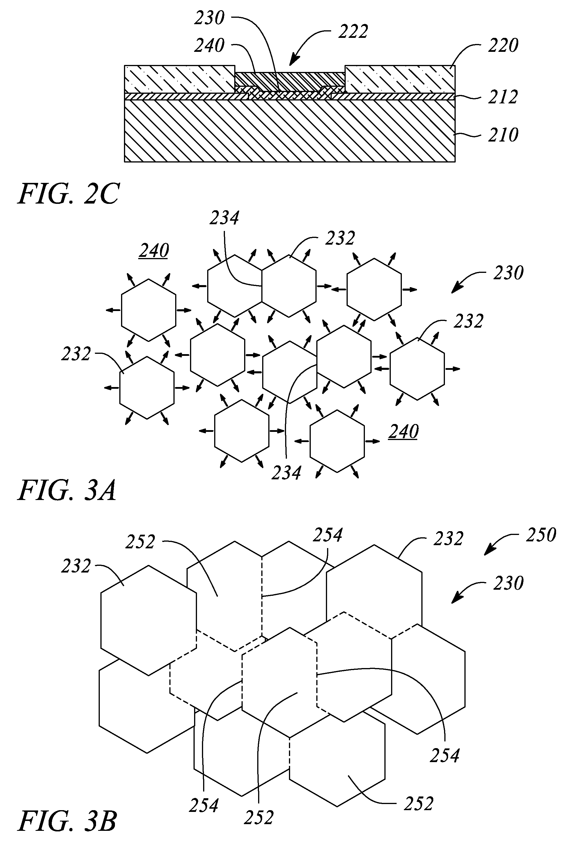
[0022]Embodiments of the present invention facilitate producing an inorganic thin film semiconductor component. For example, the inorganic thin film semiconductor component may be a channel of an enhancement mode thin film transistor (TFT). In some embodiments, the inorganic thin film semiconductor component comprises a metal-oxide semiconductor. Exemplary enhancement mode zinc oxide (ZnO) TFTs manufactured according to the present invention have exhibited high carrier mobility of approximately 100 centimeter squared per volt-second (cm2V−1s−1), high On / Off ratios of approximately 107 and low subthreshold slope performance of about 2 volts per decade (V / decade). The performance of the exemplary TFTs generally exceeds that of TFTs based on organic semiconductors as well as those that employ either an amorphous or a polycrystalline thin film semiconductor component.

[0023]According to the present invention, fabrication of the inorganic thin film semiconductor component employs a liquid...


PUM

PropertyMeasurementUnit
temperaturesaaaaaaaaaa
thicknessaaaaaaaaaa

Abstract

A thin film semiconductor and a method of its fabrication use induced crystallization and aggregation of a nanocrystal seed layer to form a merged-domain layer. The nanocrystal seed layer is deposited onto a substrate surface within a defined boundary. A reaction temperature below a boiling point of a reaction solution is employed. A thin film metal-oxide transistor and a method of its production employ the thin film semiconductor as a channel of the transistor. The merged-domain layer exhibits high carrier mobility.

Description

BACKGROUND[0001]1. Technical Field[0002]The invention relates to nanotechnology. In particular, the invention relates to structures fabricated from nano-scale particles and crystals.[0003]2. Description of Related Art[0004]A thin film semiconductor is a semiconductor fabricated by depositing semiconductor material on a substrate using thin film techniques. In general, thin film semiconductors are divided into two main groups: inorganic thin film semiconductors and organic thin film semiconductors. The inorganic thin film semiconductors generally comprise an inorganic material having properties of a semiconductor. Examples of inorganic semiconductor materials include, but are not limited to, silicon (Si), germanium (Ge), gallium arsenide (GaAs), and various metal-oxides (e.g., zinc oxide—ZnO). Organic thin film semiconductors comprise an organic material such as a polymer, an oligomer, or similar molecules that exhibit semiconductor properties. In some instances, the organic thin fil...

Claims


Application Information

Patent Timeline
Patent Type & Authority Applications(United States)
IPC IPC(8): H01L29/786H01L21/84
CPCB82Y10/00H01L29/0665H01L29/0673H01L27/1292H01L29/78696H01L29/66969Y10S977/892H01L29/7869
Inventor PAN, ALFRED I-TSUNGNG, HOU T.
Owner HEWLETT PACKARD DEV CO LP
Why Eureka
Try Eureka