Method of forming thin film for improved productivity

a thin film and productivity technology, applied in the direction of cleaning using liquids, coatings, chemistry apparatus and processes, etc., can solve the problems of large loss in production yield, contaminated by impurities in the atmosphere, unsatisfactory thin film formation, etc., to increase the manufacturing productivity of semiconductor devices, shorten the process time, and increase the cleaning period of the process chamber

Active Publication Date: 2005-06-16
SAMSUNG ELECTRONICS CO LTD
View PDF10 Cites 320 Cited by
  • Summary
  • Abstract
  • Description
  • Claims
  • Application Information

AI Technical Summary

Benefits of technology

[0011] The present invention is directed to a method of forming a thin film, capable of continuously treating a number of semiconductor substrates and increasing a cleaning period of a process chamber by suppressing particles stripped fro...

Problems solved by technology

One of the problems associated with the thin film formation process is that an undesired thin film may be formed on the inner walls of a process chamber where the thin film formation process is being performed to form a process thin film on a semiconductor substrate.
However, this wet cleaning process requires much down time, thereby causing a large loss in the production yield.
Further, since the inside of the process chamber is exposed to the atmosphere, it may be contaminated by impurities in the atmosphere.
H...

Method used


Image

  • Method of forming thin film for improved productivity
  • Method of forming thin film for improved productivity
  • Method of forming thin film for improved productivity

Examples


Embodiment Construction

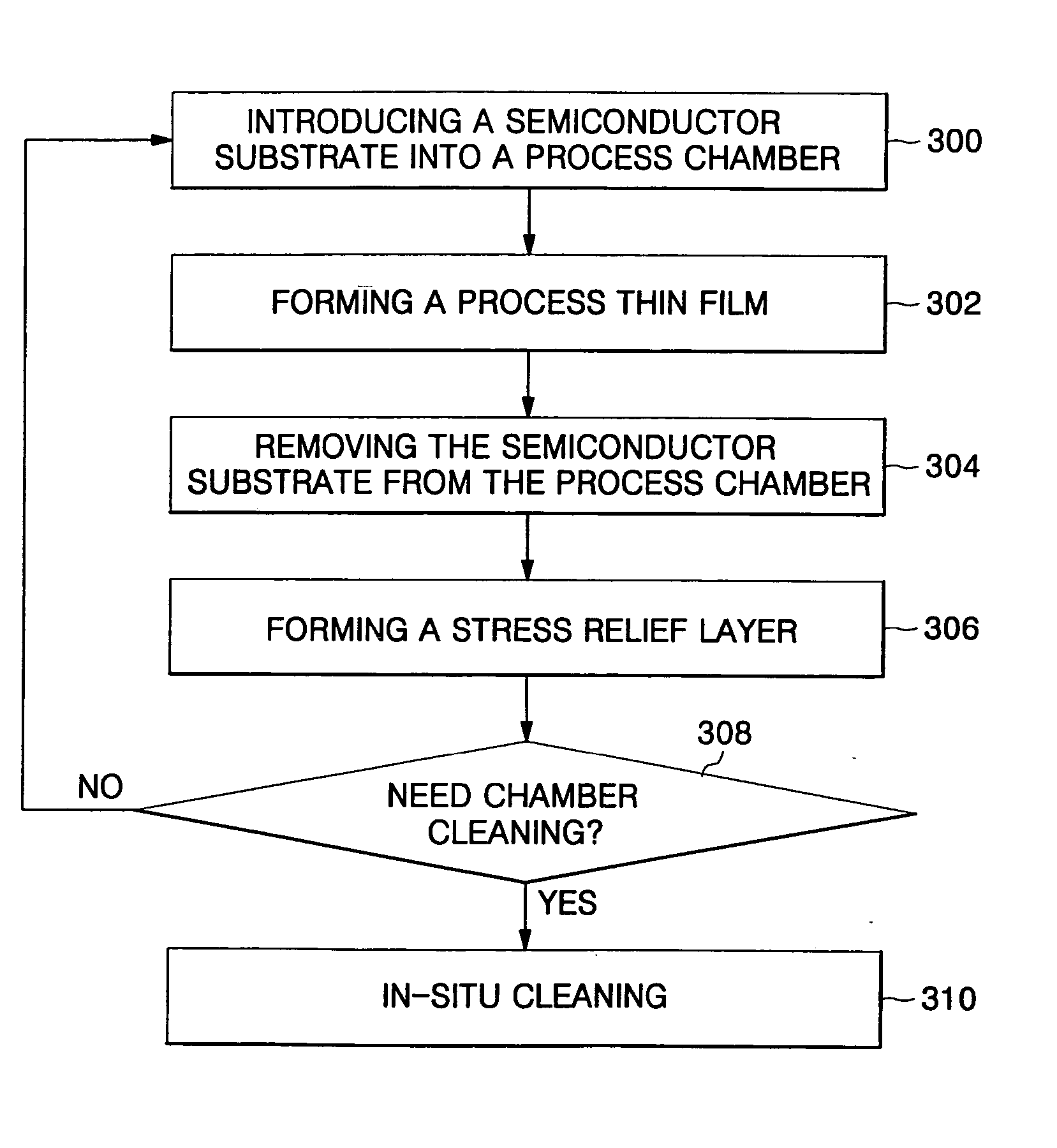
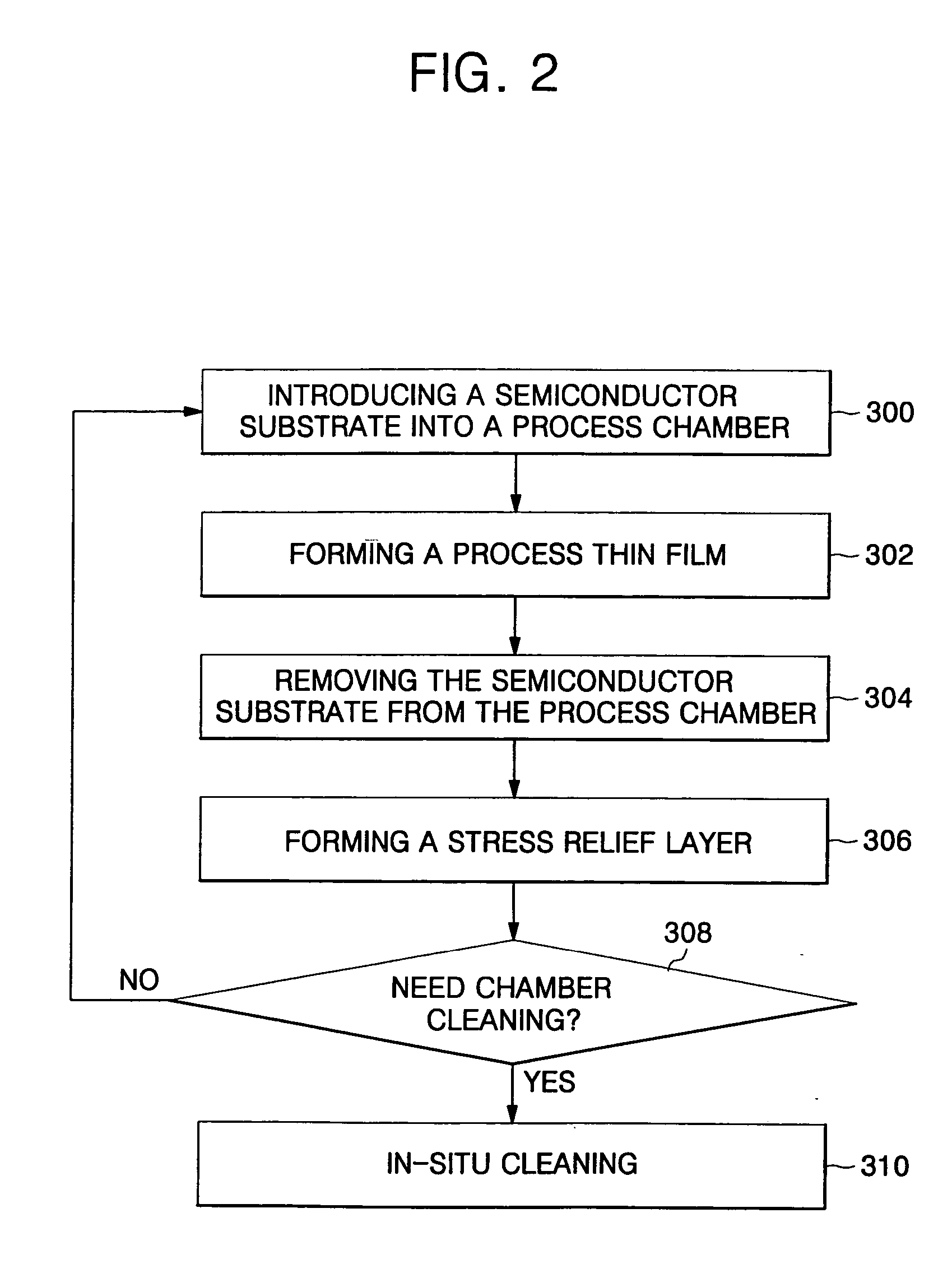
[0024]FIG. 2 is a flow chart illustrating a method of forming thin films according to embodiments of the present invention. Referring to FIG. 2, a semiconductor substrate is introduced into a process chamber (step 300). Then, a process thin film is formed on the semiconductor substrate (step 302). While the process thin film is formed on the semiconductor substrate, a chamber coating layer is formed on the inner walls of the process chamber. The chamber coating layer is the same film as the process thin film. In the embodiments of the present invention, the process thin film and the chamber coating layer may be hafnium oxide layers formed by an ALD method. Then, the semiconductor substrate on which the process thin film is formed is removed from the process chamber (step 304). Then, in the state that the semiconductor substrate is removed from the process chamber, a stress relief layer is formed on the chamber coating layer (step 306).

[0025] The stress relief layer according to one...


PUM

PropertyMeasurementUnit
Thicknessaaaaaaaaaa
Dielectric polarization enthalpyaaaaaaaaaa
Stress optical coefficientaaaaaaaaaa

Abstract

There is provided a method of forming a thin film for providing improved fabrication productivity. The method includes introducing a semiconductor substrate into a process chamber. A process thin film is formed on the semiconductor substrate, in which a chamber coating layer is formed on inner walls of the process chamber while the process thin film is formed. The semiconductor substrate is removed from the process chamber. A stress relief layer is formed on the chamber coating layer. After all of the above operations are repeatedly performed at least one time, an in-situ cleaning is performed on the chamber coating layer and the stress relief layer, which are alternately formed in stack on the inner walls of the process chamber.

Description

CROSS-REFERENCE TO RELATED APPLICATION [0001] This application claims the benefit of Korean Patent Application No. 2003-90400, filed Dec. 11, 2003, the contents of which are hereby incorporated herein by reference in their entirety. BACKGROUND [0002] 1. Technical Field [0003] The present invention relates to a method of fabricating semiconductor devices and, more particularly, to a method of forming a thin film for providing improved fabrication productivity. [0004] 2. Discussion of the Related Art [0005] The fabrication of semiconductor devices involves many processes for forming various kinds of thin films. For example, a dielectric layer such as a silicon oxide layer (SiO2), a silicon nitride layer (SiN), a hafnium oxide layer (HfO2), an aluminum oxide layer (Al2O3), and the like is used for a gate oxide layer, an insulating spacer, an etch stop layer, a capacitor dielectric layer, and the like. Further, a conductive layer such as a polysilicon layer, a tungsten layer, an aluminu...

Claims


Application Information

Patent Timeline
IPC IPC(8): H01L21/304C23C16/44H01L21/302H01L21/314H01L21/316H01L21/461
CPCC23C16/4404H01L21/31637H01L21/3141C23C16/4405H01L21/0228H01L21/02183H01L21/304
Inventor WON, SEOK-JUNKIM, WEON-HONGKWON, DAE-JIN
Owner SAMSUNG ELECTRONICS CO LTD
Why Eureka
Try Eureka