

Method for forming thin film
a thin film and manufacturing method technology, applied in the field of semiconductor manufacturing, can solve the problems of unfavorable contaminant particle formation, uneven surface, and difficult use of the pvd method for forming thin films with uniform thickness on a surface with deep trenches, so as to reduce contaminant particles and increase the deposition rate of thin films
- Summary
- Abstract
- Description
- Claims
- Application Information
AI Technical Summary
Benefits of technology
Problems solved by technology
Method used
Image

Examples
example 2-b
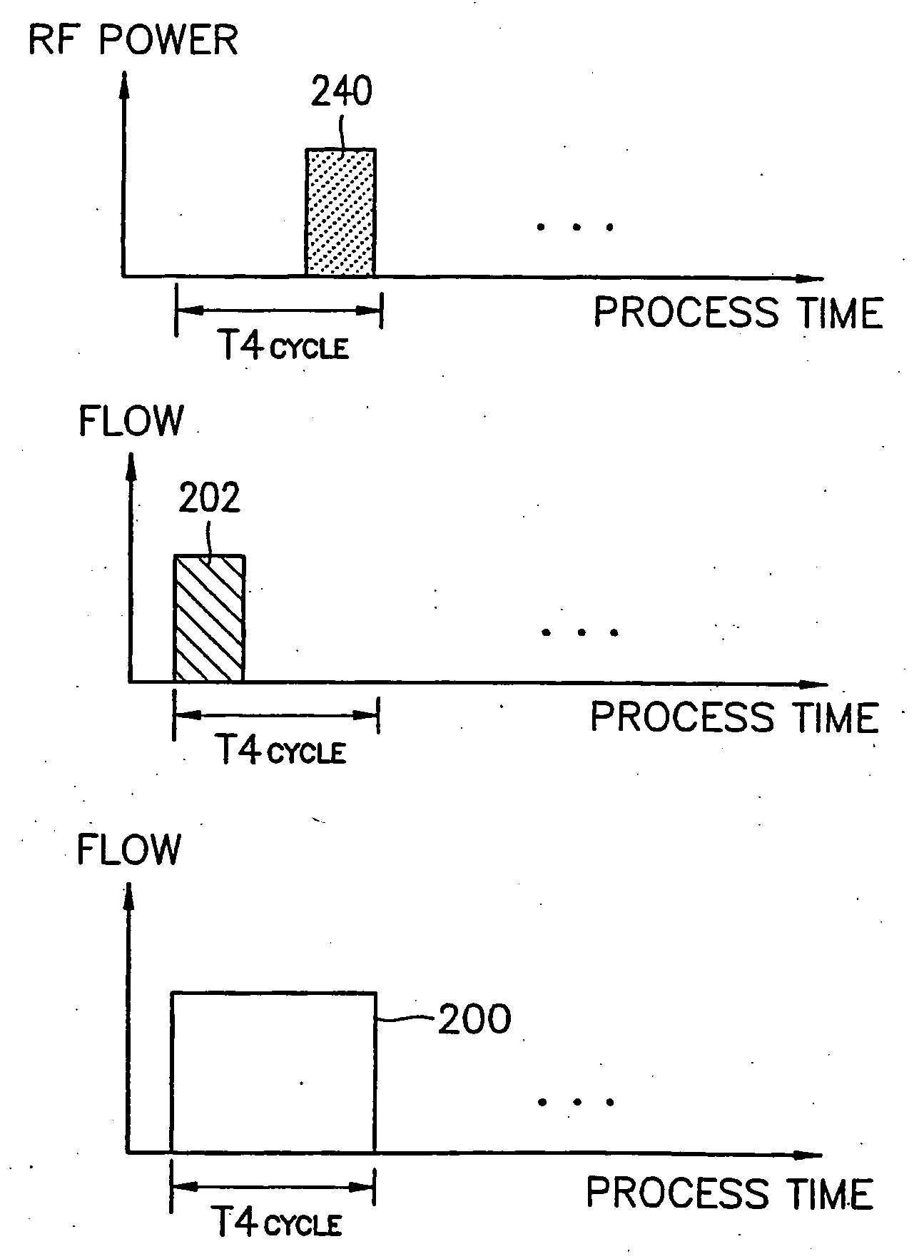
[0058] In accordance with the method for forming a thin film in Embodiment 2 described above, a titanium(Ti) film was formed. Referring to FIG. 3C, a source gas container 200 containing titaniumchloride [TiCl4] gas heated at 50° C. is connected to said reactor 230 through a first gas supply tube 214 and a valve 212 in such a way that the supply of said titaniumchloride [TiCl4] gas is controlled. The pressure of said reactor 230 is maintained at 3 Torr and the temperature of said substrate (not shown) inside said reactor 230 is also maintained at 380° C., and also 330 sccm of argon(Ar) gas and 100 sccm of hydrogen(H2) gas are supplied to said reactor 230 continuously through said main supply tube 210, and at the same time, said titaniumchloride [TiCl4] source gas is supplied for 0.2 second, and 2 seconds later, an RF power 240 at the frequency of 13.56 MHz and at the level of 200 watts is applied for 2 seconds, and the RF power 240 is turned off, and then, after 1.8 seconds said tita...
PUM
| Property | Measurement | Unit |
|---|---|---|
| size | aaaaa | aaaaa |
| thickness | aaaaa | aaaaa |
| temperature | aaaaa | aaaaa |
Abstract
Description
Claims
Application Information