Method of forming crystallographically stabilized doped hafnium zirconium based films

Active Publication Date: 2008-09-25
TOKYO ELECTRON LTD
View PDF10 Cites 371 Cited by
  • Summary
  • Abstract
  • Description
  • Claims
  • Application Information

AI Technical Summary

Benefits of technology

[0007]Embodiments of the invention provide a method for forming crystallographically stabilized doped hafnium zirconium based films by atomic layer deposition (ALD) and plasma enhanced ALD (PEALD). The doped hafnium zirconium based films include oxide, nitride, and oxynitride films that further contain one or more dopant elements selected from Group II, Group XIII, silicon, a

Problems solved by technology

While HfO2 and ZrO2 mixtures have exhibited improved properties, conventional CMOS technology has not successfully utilized HfO2 and ZrO2 mixtures because the combinatio

Method used


Image

  • Method of forming crystallographically stabilized doped hafnium zirconium based films
  • Method of forming crystallographically stabilized doped hafnium zirconium based films
  • Method of forming crystallographically stabilized doped hafnium zirconium based films

Examples


Embodiment Construction

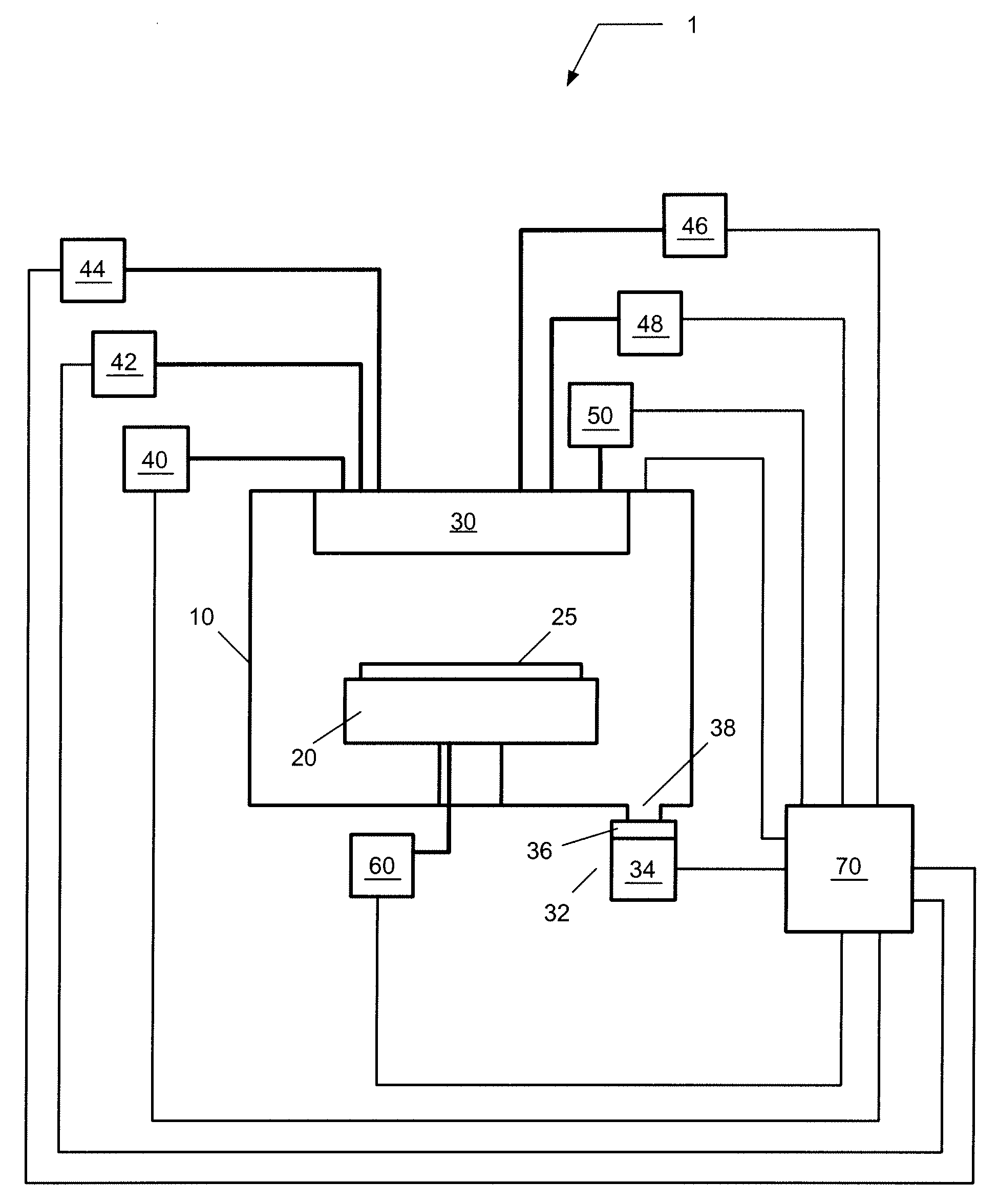
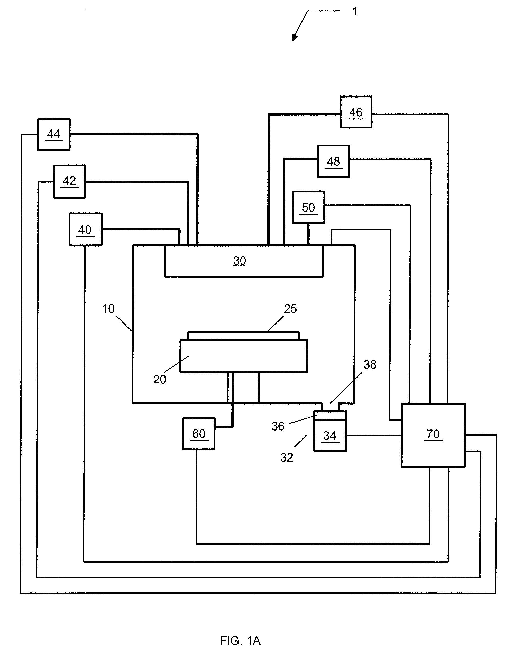
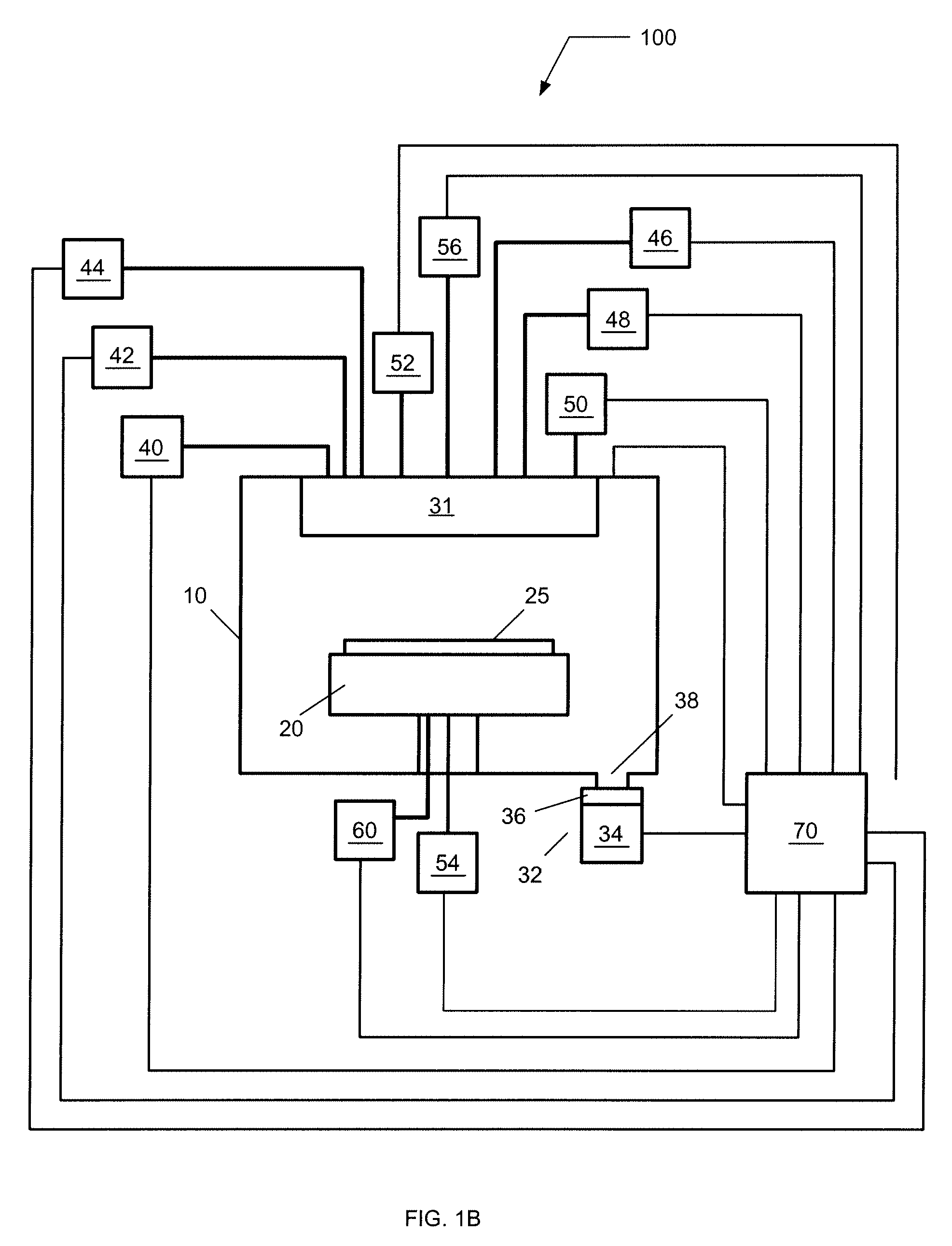
[0019]Doped hafnium zirconium based materials can provide beneficial thermal and electrical characteristics for semiconductor applications. Because hafnium and zirconium are chemically similar and practically infinitely miscible as oxides, nitrides, and oxynitrides, they form highly stable solid solutions. Benefits of films containing doped hafnium zirconium based materials include increased thermal stability in contact with silicon or metal gate electrode material, increased crystallization temperature, increased dielectric constant of the doped hafnium zirconium oxide material compared to hafnium oxide, decreased density of interface traps, decreased threshold voltage shifts and Fermi level pinning, and improved processing characteristics.

[0020]ZrO2 and HfO2 can both form monoclinic, tetragonal, and cubic polymorphs (crystallographic forms) but it has been shown that the cubic form is the most stable form at typical semiconductor processing temperatures. Calculations indicate that...


PUM

PropertyMeasurementUnit
Thicknessaaaaaaaaaa

Abstract

A method is provided for forming doped hafnium zirconium based films by atomic layer deposition (ALD) or plasma enhanced ALD (PEALD). The method includes disposing a substrate in a process chamber and exposing the substrate to a gas pulse containing a hafnium precursor, a gas pulse containing a zirconium precursor, and a gas pulse containing one or more dopant elements. The dopant elements may be selected from Group II, Group XIII, silicon, and rare earth elements of the Periodic Table. Sequentially after each precursor and dopant gas pulse, the substrate is exposed to a gas pulse containing an oxygen-containing gas, a nitrogen-containing gas, or an oxygen- and nitrogen-containing gas. In alternative embodiments, the hafnium and zirconium precursors may be pulsed together, and either or both may be pulsed with the dopant elements. The sequential exposing steps may be repeated to deposit a doped hafnium zirconium based film with a predetermined thickness.

Description

CROSS-REFERENCE TO RELATED APPLICATIONS[0001]This application is related to co-pending U.S. patent application Ser. No. ______, (Attorney Docket No. 304155US), entitled “SEMICONDUCTOR DEVICE CONTAINING CRYSTALLOGRAPHICALLY STABILIZED DOPED HAFNIUM ZIRCONIUM BASED MATERIALS,” filed on the same date as the present application, the entire content of which is hereby incorporated by reference.FIELD OF INVENTION[0002]The present invention relates to high dielectric constant (high-k) materials for semiconductor devices, and more particularly to methods of forming crystallographically stabilized doped hafnium zirconium oxide, nitride, or oxynitride films.BACKGROUND OF THE INVENTION[0003]Conventional complimentary metal oxide semiconductor (CMOS) technology requires gate dielectric layers having higher dielectric constant than SiO2 or SiON. High-k materials such as HfO2 and ZrO2 have been investigated extensively as possible alternatives to SiO2-based options due to their relatively high die...

Claims


Application Information

Patent Timeline
IPC IPC(8): C23C16/06
CPCC23C16/308C23C16/34C23C16/45553C23C16/45531C23C16/45536C23C16/405
Inventor CLARK, ROBERT D.
Owner TOKYO ELECTRON LTD
Why Eureka
Try Eureka