Semi-conductor surface emitting laser and production method and applications thereof

A surface emitting laser, semiconductor technology, applied in semiconductor lasers, lasers, laser parts and other directions, can solve the problems of reducing device life and reliability, difficult heat dissipation, device life and stability effects, etc., to improve working life and Work reliability, improve heat dissipation performance, improve the effect of heat dissipation characteristics

Active Publication Date: 2013-07-17
WUHAN TELECOMM DEVICES
View PDF5 Cites 10 Cited by
  • Summary
  • Abstract
  • Description
  • Claims
  • Application Information

AI Technical Summary

Problems solved by technology

When the conventional 850nm surface-emitting chips currently on the market are used for space communication, the operating current must be increased very much, almost close to the saturation current. At this time, the temperature of the active layer may even exceed 170-180°C, which seriously reduces the performance of the device. life and reliability
For free communication in space with a distance of 1-3km, it is very necessary for the working power of the surface-emitting laser to reach 10-30mW. At this time, if the conventional method is used to increase the power, the power will increase by an order of magnitude. It is necessary to enlarge the oxidation hole to more than 18μm, but this will increase the size of the mesa and the capacitance value of the device, which will lead to more serious heat dissipation problems of the device, and ultimately greatly affect the reliability of the device. Therefore, it is necessary to completely re- Optimize the material, structure and process of the entire device to meet the requirements of industry technology
[0005] Existing surface-emitting lasers for optical fiber communication generally use GaAs / AlGaAs (gallium arsenide / aluminum gallium arsenide) triple quantum wells as the active region, and the upper and lower mirrors use 22 pairs and 35 pairs respectively. The DBR (distributed Bragg reflector) pair of AlGaAs with high Al (aluminum) composition and AlGaAs with low Al composition of λ / 4, among them, the use of ternary DBR pairs can indeed effectively reduce the resistance of DBR, which is small In the case of high power, the lifetime of the device can be effectively improved, but it will have a serious adverse effect on the heat dissipation of the surface emitting laser with higher power, because the heat dissipation performance of the ternary compound is lower than that of the binary compound. about three times
[0006] The application number is 200510016967.X, the application publication number is CN1719673A, and the Chinese invention patent application titled "a vertical external cavity surface emitting semiconductor laser with convex-concave mirror" discloses a heat sink, an anti-reflection coating, and The vertical external cavity surface-emitting semiconductor laser of the microchannel heat sink can use the above-mentioned components and corresponding structures to solve the heat dissipation problem of high-power semiconductor lasers to a certain extent, but because of its heat dissipation effect and effective life time, it will be relatively large It is limited by the performance index and structural technical level of the above-mentioned components, which affects the life and stability of the overall device, and it also has the defects of complex overall device structure and cumbersome manufacturing process
[0007] The application number is 201110072769.0, the application publication number is CN102694341A, and the Chinese invention patent application titled "An Etching and Heat Dissipation Enhanced Vertical Cavity Surface Emitting Laser" discloses a method to remove the corresponding substrate in the center of the substrate by etching. Thereby forming a vertical cavity surface emitting laser with substrate grooves, although it can better solve the heat dissipation problem of high-power semiconductor lasers by filling the substrate grooves of the lower motor with high thermal conductivity solder, but because of its heat dissipation The effect is greatly affected by the technical level of trench etching and high thermal conductivity solder filling technology, and even the performance index of high thermal conductivity solder itself, which leads to the corresponding impact on the life and stability of the overall device. At the same time, its There are also defects of increasing the complexity of the overall device structure, increasing the difficulty of the device manufacturing process, and increasing the cost of device manufacturing
[0008] Generally speaking, in the free space communication of some existing semiconductor surface-emitting lasers with a distance of 1-3km, there are many defects that the heat dissipation problem is difficult to solve ideally under high-power working conditions, so the overall device life is short , poor stability, complex overall device structure, complex and difficult device manufacturing process, and high device processing costs, it is difficult to meet the needs of practical applications of space free communication

Method used


Image

  • Semi-conductor surface emitting laser and production method and applications thereof
  • Semi-conductor surface emitting laser and production method and applications thereof
  • Semi-conductor surface emitting laser and production method and applications thereof

Examples


Embodiment 1

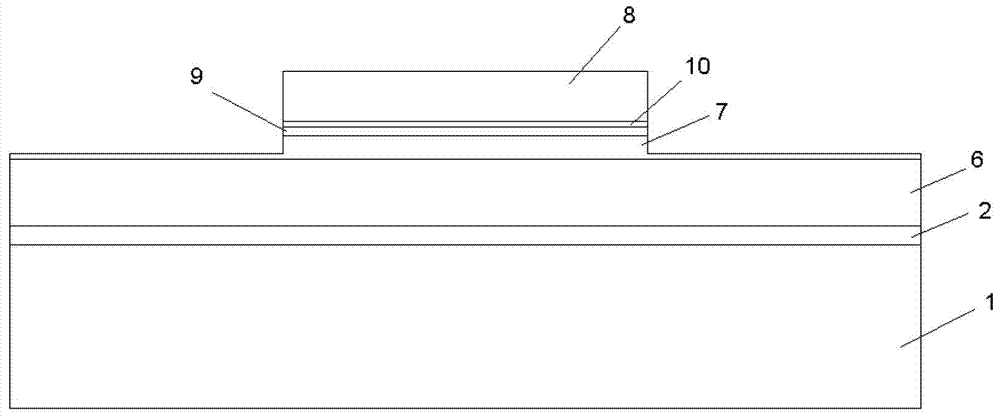
[0049] A semiconductor surface-emitting laser, comprising a sequentially connected substrate layer 1, an N-type GaAs buffer layer 2, a lower distributed Bragg reflector DBR layer 6, an upper layer 7 of the lower distributed Bragg reflector DBR layer, and an active layer 9 , an oxidized current confinement layer 10 and an upper DBR layer 8; the buffer layer 2 is provided with an N-type electrode 4, and the upper DBR layer 8 is provided with a P-type electrode 12; the oxidized current confinement layer 10 is provided with There is a light outlet 11; the lower DBR layer 6 uses binary N-type AlAs / GaAs pairs; the number of binary N-type AlAs / GaAs pairs in the lower distributed Bragg reflector DBR layer 6 is thirty pairs; the The diameter of the light exit hole 11 is 14-18 μm; the upper layer of the lower distributed Bragg reflector DBR layer 6 is a ternary N-type distributed Bragg reflector DBR layer, and the upper distributed Bragg reflector DBR layer 8 is three Element P-type dis...

Embodiment 2

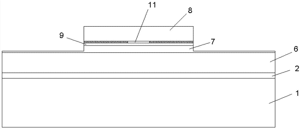
[0051] A semiconductor surface-emitting laser, comprising a substrate layer 1, a buffer layer 2, a lower distributed Bragg reflector DBR layer 6, an upper layer 7 of the lower distributed Bragg reflector DBR layer, an active layer 9, an oxidized The current confinement layer 10 and the upper distributed Bragg reflector DBR layer 8; the buffer layer 2 is provided with an N-type electrode 4, and the upper distributed Bragg reflector DBR layer 8 is provided with a P-type electrode 12; the oxidation The current confinement layer 10 is provided with a light exit hole 11; the diameter of the light exit hole 11 is 14-18 μm; the lower distributed Bragg reflector DBR layer 6 uses a binary N-type AlAs / GaAs pair; the lower distributed The number of binary N-type AlAs / GaAs pairs in the DBR layer 6 of the Bragg reflector is thirty pairs; well; the entire thickness of the active layer 9 is a length of λ; the substrate layer 1 is a semi-insulating GaAs substrate layer; the buffer layer 2 is ...

Embodiment 3

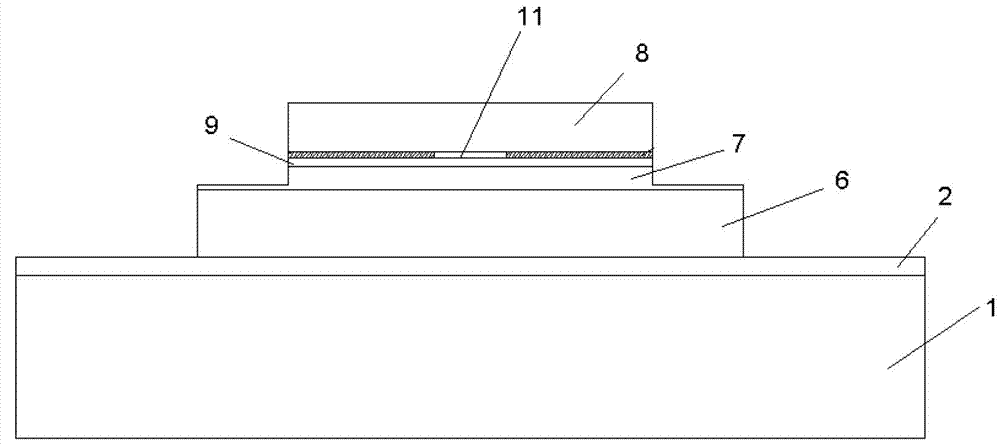
[0053] A semiconductor surface-emitting laser, comprising a substrate layer 1, a buffer layer 2, a lower distributed Bragg reflector DBR layer 6, an upper layer 7 of the lower distributed Bragg reflector DBR layer, an active layer 9, an oxidized A current confinement layer 10 and an upper DBR layer 8; the buffer layer 2 is provided with an N-type electrode 4, and the upper distributed Bragg reflector DBR layer 8 is provided with a P-type electrode 12; the oxidized current confinement layer 10 A light exit hole 11 is provided on the top; the diameter of the light exit hole 11 is 14-18 μm; the lower DBR layer 6 adopts a binary N-type AlAs / GaAs pair; the binary N-type AlAs / GaAs pair of the lower DBR layer 6 The number is thirty pairs; the buffer layer 2, the lower distributed Bragg reflector DBR layer 6, the upper layer 7 of the lower distributed Bragg reflector DBR layer, the active layer 9, the oxidized current confinement layer 10 and the upper distributed The upper and side s...


PUM


Abstract

The invention relates to a semi-conductor surface emitting laser and a production method and applications thereof. An active layer utilizes a strain five quantum well; a lower DBR (Distributed Bragg Reflector) layer utilizes a binary N type AlAs / GaAs pair; an upper DBR layer utilizes a DBR of a general ternary N type Al0.92Ga0.08 As/Al0.12Ga0.88As; a plurality of pairs under the active layer utilize a same structure; the top utilizes a high thermal conductive ALN (Aluminium Nitride) layer; copper layers are arranged and covered on bilateral sides of the platform surface and above the platform; the size of an oxidation hole is 18 micron; and the capacitance of components are reduced through a BCB (p-bis benzene) layer. The production method of the semi-conductor surface emitting laser has the advantages of improving an integral heat dissipation level by improving processes, effectively solving the heat dissipation problem of a large power surface emitting laser, improving an stage of the power of the surface emitting laser, enabling the surface emitting laser to be improved in material character, improving the service life and working reliability of the surface emitting laser and achieving free space communication within 1-3 km.

Description

technical field [0001] The invention belongs to the technical field of semiconductor light-emitting devices and preparation methods thereof, and relates to a semiconductor surface-emitting laser and a preparation method thereof, in particular to a semiconductor surface-emitting laser suitable for free space communication, a preparation method and an application thereof. Background technique [0002] In the research and application of optical fiber transmission technology, due to the small threshold current, small divergence angle and circular spot of the short-wavelength surface-emitting laser, it can realize high-speed modulation in a short distance, and has the characteristics of energy saving and environmental protection. More and more attention and development. [0003] At present, the research on surface-emitting lasers is mainly focused on the high-speed technology of milliwatt-level low-power devices for optical communication applications, including the 850nm short-di...

Claims


Application Information

Patent Timeline
Patent Type & Authority Applications(China)
IPC IPC(8): H01S5/343H01S5/187H01S5/024
Inventor 汤宝余向红岳爱文王任凡
Owner WUHAN TELECOMM DEVICES
Why Eureka
Try Eureka