Double-sided microchannel liquid-cooled power semiconductor whole-wafer flat-panel crimp package structure

A power semiconductor and micro-channel technology, applied in semiconductor devices, semiconductor/solid-state device components, electric solid-state devices, etc., can solve the problems of increased heat generation failure rate, large volume, and reduced contact area, and achieve long-term improvement. Reliability, high integratable power, avoidance of contact gap effect

Inactive Publication Date: 2017-05-03
NANJING HIGHSEMI ELECTRIC POWER SCI & TECH CO LTD
View PDF5 Cites 0 Cited by
  • Summary
  • Abstract
  • Description
  • Claims
  • Application Information

AI Technical Summary

Problems solved by technology

[0003] 1. Ordinary power semiconductor packaging occupies a large volume, and a large amount of lead bonding is required when packaging, which brings parasitic inductance and parasitic capacitance, thereby increasing heat generation and improving failure rate, and is limited by the current that a single chip can pass The limit cannot bear more current;
[0004] 2. The traditional heat sink structure cannot meet the heat dissipation requirements in high-power devices, and requires a larger heat sink structure or a water-cooled structure, while the conventional water-cooled structure is bulky;
[0005] 3. In the traditional flat crimping packaging structure, the crimping material on the wafer surface is mostly made of hard metal materials. In order to ensure the flat contact with the wafer surface, extreme requirements are put forward for the flatness and roughness of the crimping material surface. High requirements, and extremely strict requirements on the crimping force during packaging, resulting in difficulties in processing and assembly; defects in the processing and assembly process will reduce the contact area, increase the current density per unit area, and increase the thermal resistance. reliability

Method used


Image

  • Double-sided microchannel liquid-cooled power semiconductor whole-wafer flat-panel crimp package structure
  • Double-sided microchannel liquid-cooled power semiconductor whole-wafer flat-panel crimp package structure
  • Double-sided microchannel liquid-cooled power semiconductor whole-wafer flat-panel crimp package structure

Examples


Embodiment Construction

[0024] Embodiments of the present invention are further described below in conjunction with the accompanying drawings:

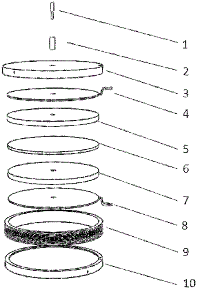
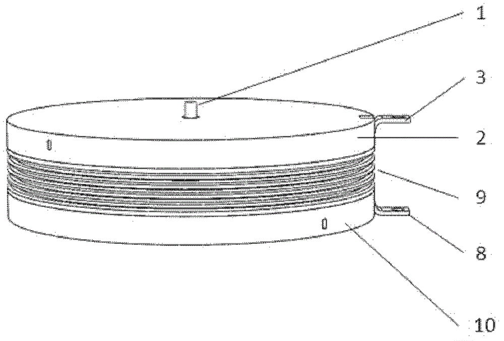
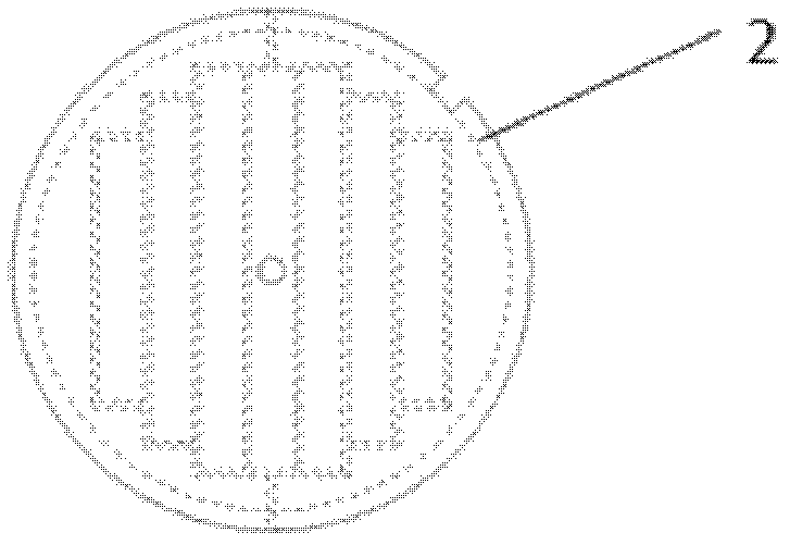
[0025] Known power semiconductor wafers usually contain tens to hundreds of identical semiconductor chips, and each chip is composed of thousands of identical units connected in parallel, and the emitter, gate and collector of each unit are connected through Metal or polysilicon films are connected together respectively. However, in the actual manufacturing process, it is difficult to ensure that every tiny unit on a complete wafer is completely qualified, and if unqualified units continue to be used, the entire wafer will fail. Therefore, if there are a small number of unqualified units when manufacturing wafers, they can be isolated during the manufacturing process, and the failure area is marked on the surface of the wafer, and then a polymer insulation pattern is prepared on the corresponding part of the graphite sheet to disconnect the failure area , w...


PUM


Abstract

Provided is a liquid-cooled power semiconductor wafer plate crimping packaging structure with micro channels on double surfaces. The plate crimping packaging structure comprises a power semiconductor wafer, a spring needle, graphite flakes, an emitter electrode metallic sheet, a collector electrode metallic sheet, a top cooling plate, a bottom cooling plate, and a ceramic tube housing. Graphite flakes are pressed on the top surface and the bottom surface of the wafer. The emitter electrode metallic sheet is arranged on the graphite flake to be used as a leading out terminal for leading out the collector electrode of the wafer, while the collector electrode metallic sheet is arranged on the graphite flake to be used as a leading out terminal for leading out the emitter electrode of the wafer. The graphite flakes, the emitter electrode metallic sheet, and the collector electrode metallic sheet are sealed in the ceramic tube housing. The top cooling plate is pressed on the top of the ceramic tube housing, while the bottom cooling plate is pressed on the bottom of the ceramic tube housing. Cooling micro channels are disposed on the top cooling plate and the bottom cooling plate. The spring needle is pressed on the central position of the top cooling plate in order to lead out the gate electrode of the wafer. The plate crimping packaging structure has advantages of achieving connection without leading wires, reducing stray inductance and stray capacitance generated by leading wire bonding, and increasing a current conducting capability, heat conducting capability, an anti-thermal-shock capability, and reliability, and advantages of a small structural size, a high heat dissipating coefficient, a long service life, and an intelligent monitoring function.

Description

technical field [0001] The invention relates to a semiconductor device, in particular to a double-sided microchannel liquid-cooled power semiconductor whole wafer flat crimping packaging structure. Background technique [0002] Semiconductor devices, especially high-power semiconductor devices, are widely used in the field of electronic power. With the development of power semiconductors, how to reduce the weight and volume of power semiconductors and solve the heat dissipation problems caused by the consequent high power density has attracted widespread attention in the industry. The press-fit packaging form of semiconductor devices and efficient cooling structure design become the key factors for reducing the weight and volume of devices. Existing high-power semiconductor devices have the following deficiencies: [0003] 1. Ordinary power semiconductor packaging occupies a large volume, and a large amount of lead bonding is required when packaging, which brings parasitic...

Claims


Application Information

Patent Timeline
Patent Type & Authority Patents(China)
IPC IPC(8): H01L23/473
CPCH01L2924/0002
Inventor 刘胜吴林徐玲周洋陈明祥
Owner NANJING HIGHSEMI ELECTRIC POWER SCI & TECH CO LTD
Why Eureka
Try Eureka