
Packaging structure of single-chip bidirectional IGBT module

A packaging structure, single-chip technology, applied in electrical components, electrical solid devices, circuits, etc., can solve the problems of reducing parasitic parameters of modules, welding interface thermo-mechanical fatigue failure, etc., to reduce parasitic parameters, improve thermal conductivity and Power density, effect of shortening distance

Inactive Publication Date: 2016-07-20
HUNAN UNIV +1
View PDF1 Cites 3 Cited by
  • Summary
  • Abstract
  • Description
  • Claims
  • Application Information

AI Technical Summary

Problems solved by technology

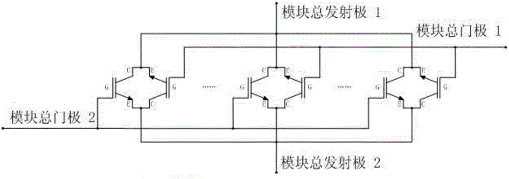
[0008] The technical problem to be solved by the present invention is to provide a packaging structure of a single-chip bidirectional IGBT module, realize double-sided heat dissipation of the single-chip bidirectional IGBT module, improve the power density of the module; cancel the metal bonding wire for interconnection, reduce The parasitic parameters of the module; solve the problem of thermomechanical fatigue failure of the metal bonding wire and its welding interface, and improve the current impact resistance and reliability of the module

Method used


Image

  • Packaging structure of single-chip bidirectional IGBT module
  • Packaging structure of single-chip bidirectional IGBT module
  • Packaging structure of single-chip bidirectional IGBT module

Examples


Embodiment Construction

[0036] Embodiments of the present invention will be further described in detail below in conjunction with the accompanying drawings and examples. The following examples are used to illustrate the present invention, but should not be used to limit the scope of the present invention.

[0037] In the description of the present invention, it should be noted that unless otherwise specified, the meaning of "plurality" is two or more; the terms "upper", "lower", "left", "right", "inner ", "outside", "front end", "rear end", "head", "tail", etc. indicate the orientation or positional relationship based on the orientation or positional relationship shown in the drawings, and are only for the convenience of describing the present invention and Simplified descriptions, rather than indicating or implying that the device or element referred to must have a particular orientation, be constructed and operate in a particular orientation, and thus should not be construed as limiting the inventi...


PUM


Abstract

The invention relates to a packaging structure of a single-chip bidirectional IGBT module. The packaging structure comprises a bottom metal plate, a bottom DBC plate, a single-chip bidirectional IGBT device, a top DBC plate and a top metal plate. The bottom DBC plate comprises a second gate electrode copper clad region and a second emission electrode copper clad region. The second gate electrode and the second emission electrode of the single-chip bidirectional IGBT device are respectively connected with the second gate electrode copper clad region and the second emission electrode copper clad region. The top DBC plate comprises a first gate electrode copper clad region and a first emission electrode copper clad region. The electrodes of the upper and lower surfaces of the single-chip bidirectional IGBT device are respectively welded on the two DBC plates, and metal bonding line interconnection is replaced by welding interconnection so that the problem of thermal mechanical fatigue failure of metal bonding lines and the welding interface thereof can be solved, and current surge resistant capacity and reliability of the module can be enhanced; meanwhile, interconnection distance between external pins and the electrodes can be shortened by welding interconnection in comparison with that of metal bonding line interconnection so that the parasitic parameters of the module can be reduced.

Description

technical field [0001] The invention relates to the field of semiconductor manufacturing, in particular to a package structure of a single-chip bidirectional IGBT module. Background technique [0002] At present, insulated gate bipolar transistor (IGBT) is a power electronic device that combines the advantages of metal-oxide-semiconductor field effect transistor (MOSFET) and bipolar junction transistor. IGBT has been widely used for its excellent performance. applications, greatly improving the performance of power electronic devices and systems. Traditional AC-DC-AC converters (AC-DC-AC converters) require large-capacity capacitors to maintain the stable operation of the intermediate DC link (DC link), which makes the converter larger in size and weight. In addition, compared with power devices, the service life of capacitors is obviously insufficient, which affects the reliability and service life of the converter. The AC-AC converter (AC-AC converter) eliminates the int...

Claims


Application Information

Patent Timeline
IPC IPC(8): H01L29/739H01L23/367H01L23/492
CPCH01L29/7393H01L23/367H01L23/492
Inventor 曾重敖杰王俊沈征
Owner HUNAN UNIV
Learn More