Systems, Methods, and Apparatuses for High Power Complementary Metal Oxide Semiconductor (CMOS) Antenna Switches Using Body Switching and Substrate Junction Diode Controlling in Multistacking Structure

a technology of metal oxide semiconductor and antenna switch, which is applied in the direction of antenna support/mounting, pulse technique, antennas, etc., can solve the problems of rf switch, current cmos technology presents a variety of difficulties, and cmos technology is used for rf switch, so as to achieve high power handling capability, lower leakage current, and high power blocking capability

Inactive Publication Date: 2008-06-05
SAMSUNG ELECTRO MECHANICS CO LTD +1
View PDF23 Cites 24 Cited by
  • Summary
  • Abstract
  • Description
  • Claims
  • Application Information

AI Technical Summary

Benefits of technology

[0006]Embodiments of the invention may provide for CMOS radio frequency (RF) switches, which may be referred to as a CMOS SPDT switch. According to an embodiment of the invention, the CMOS RF switch may be fabricated using a standard 0.18 um process, although other processes may be utilized without departing from embodiments of the invention. In order to provide high power handling capability in a multi-band operation (e.g., about 900 MHz, 1.9 GHz, 2.1 GHz, etc.) of the CMOS RF switch, multi-stacked transistors with substrate body switching and source or drain-to-bulk connection may be applied to the receiver switch. According to an embodiment of the invention, the CMOS RF switch may provide higher power blocking capability and lower leakage current toward the receiver switch at the transmission (Tx) mode as well as low insertion loss at the reception (Rx) mode at multi-band (e.g., 900 MHz, 1.9 GHz, 2.1 GHz, and the like).

Problems solved by technology

Two significant mobile application components—power amplifiers (PAs) and radio frequency (RF) switches—have not yet been commercially integrated into CMOS technology.
However, current CMOS technology presents a variety of difficulties for its application to RF switches.
In particular, CMOS material characteristics, including lossy substrates due to low mobility of electrons and low breakdown voltages due to p-n junction, hot carrier effects, have prevented CMOS technology from being used for RF switches that require multi-band operation, high power levels, and / or integration with other devices and circuits.

Method used


Image

  • Systems, Methods, and Apparatuses for High Power Complementary Metal Oxide Semiconductor (CMOS) Antenna Switches Using Body Switching and Substrate Junction Diode Controlling in Multistacking Structure
  • Systems, Methods, and Apparatuses for High Power Complementary Metal Oxide Semiconductor (CMOS) Antenna Switches Using Body Switching and Substrate Junction Diode Controlling in Multistacking Structure
  • Systems, Methods, and Apparatuses for High Power Complementary Metal Oxide Semiconductor (CMOS) Antenna Switches Using Body Switching and Substrate Junction Diode Controlling in Multistacking Structure

Examples


second embodiment

[0037]II. a CMOS RF Antenna Switch

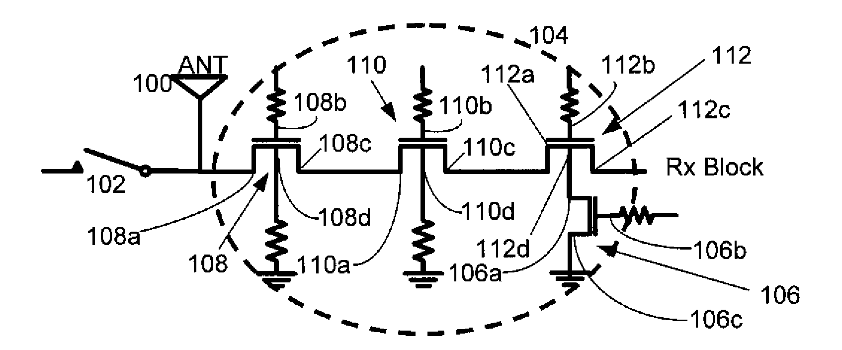
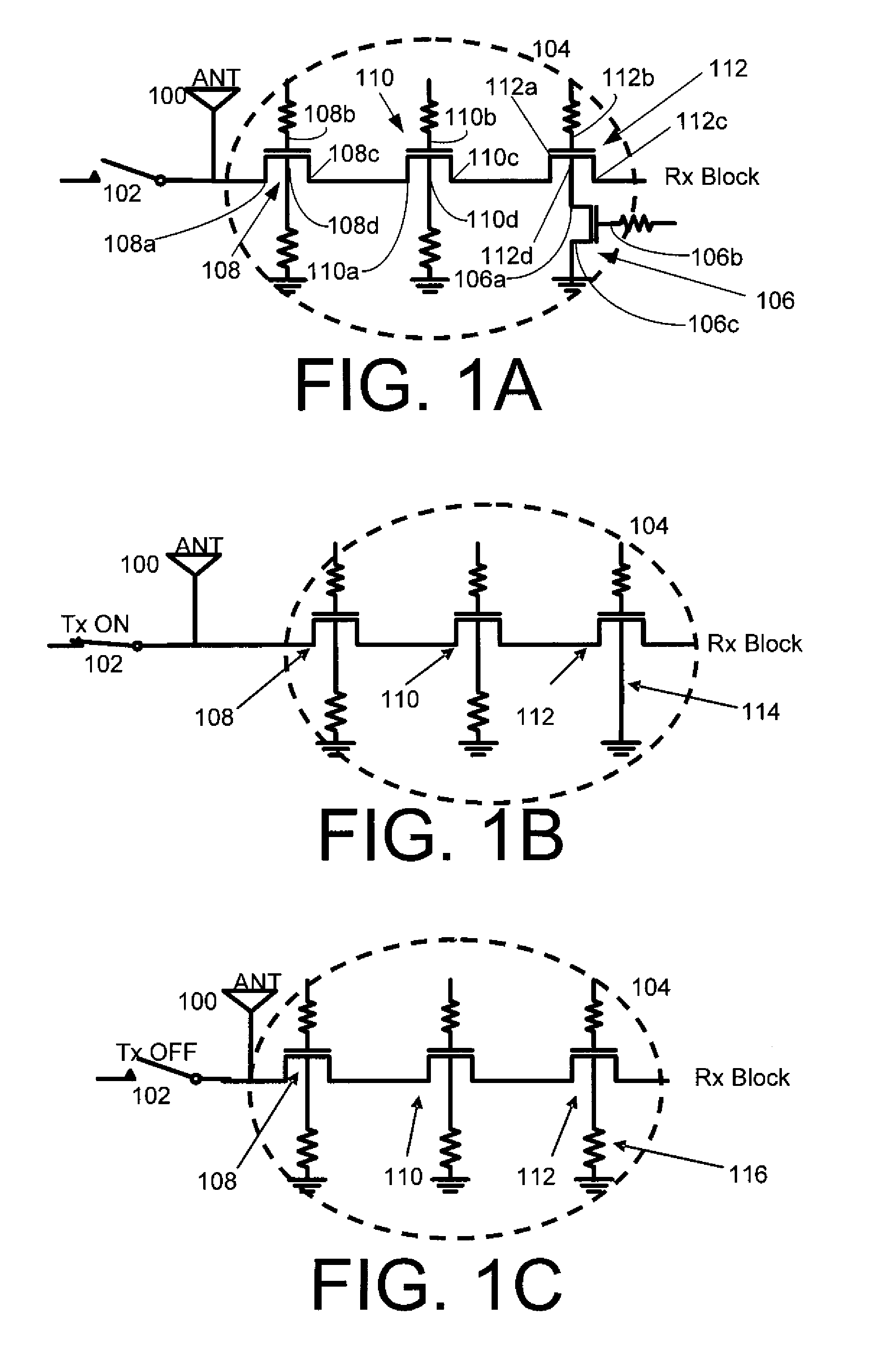
[0038]An alternative embodiment of a CMOS RF antenna switch with additional harmonic performance and / or power handling capability will now be discussed with reference to FIGS. 4A-4C and 5. Generally, a CMOS RF antenna switch in accordance with an example embodiment of the invention may include source-to-bulk or drain-to-bulk electrical connections.

[0039]FIG. 4A illustrates simplified operations of another example receiver switch 404 in accordance with an embodiment of the invention. In particular, the receiver switch 400 may include cascaded or stacked transistors 408, 140, 142, and 406, which may be CMOS transistors, according to an example embodiment of the invention. The transistor 408 may include a source 408a, a gate 408b, a drain 408c, and a body substrate 408d. The transistor 410 may include a source 410a, a gate 410b, a drain 410c, and a body substrate 410d. The transistor 412 may include a source 412a, a gate 412b, a drain 412c, and a body ...


PUM


Abstract

Embodiments of the invention may provide for a CMOS antenna switch, which may be referred to as a CMOS SPDT switch. The CMOS antenna switch may operate at a plurality of frequencies, perhaps around 900 MHz 1.9 GHz and 2.1 GHz according to an embodiment of the invention. The CMOS antenna switch may include both a receiver switch and a transmit switch. The receiver switch may utilize a multi-stack transistor with body substrate switching and source and body connection along with body floating technique to block high power signals from the transmit path by preventing channel formation of the device in OFF state as well as to maintain low insertion loss at the receiver path. Example embodiments of the CMOS antenna switch may provide for 35 dBm P 1 dB at both bands (e.g., 900 MHz and 1.9 GHz and 2.1 GHz). In addition, a −60 dBc second and third harmonic up to 28 dBm input power to the switch, may be obtained according to example embodiments of the invention.

Description

RELATED APPLICATION[0001]The present application claims priority to U.S. Provisional Application No. 60 / 868,172, filed Dec. 1, 2006, and entitled “Systems, Methods, and Apparatuses for High Power Complementary Metal Oxide Semiconductor (CMOS) Antenna Switches Using Body Switching and Substrate Junction Diode Controlling in Multistacking Structure,” which is hereby incorporated by reference in its entirety.FIELD OF THE INVENTION[0002]Embodiments of the invention relate generally to antenna switches, and more particularly, to complementary metal oxide semiconductor (CMOS) antenna switches.BACKGROUND OF THE INVENTION[0003]In the past decade, the wireless communication industry has experienced explosive growth, which has in turn accelerated the development of integrated circuit (IC) industry. In particular, in the IC industry, many mobile application systems like low noise amplifiers (LNAs), mixers, and voltage-controlled oscillators (VCOs) have been integrated into CMOS technology. Two...

Claims


Application Information

Patent Timeline
Patent Type & Authority Applications(United States)
IPC IPC(8): H01Q9/04
CPCH03K17/102H04B1/48H03K2217/0018H03K17/693H01P1/15H03K17/6871H01H36/00H01Q1/24
Inventor AHN, MINSIKLEE, CHANG-HOCHANG, JAEJOONWOO, WANGMYONGKIM, HAKSUNLASKAR, JOY
Owner SAMSUNG ELECTRO MECHANICS CO LTD
Why Eureka
Try Eureka