Method for manufacturing insulating metal base plate of electronic circuit

An insulating metal and electronic circuit technology, which is used in the improvement of metal adhesion of insulating substrates, printed circuits, and printed circuit manufacturing, etc. Low cost and the effect of increasing the micro-interface area

Inactive Publication Date: 2012-10-17
苏州衡业新材料科技有限公司
View PDF3 Cites 28 Cited by
  • Summary
  • Abstract
  • Description
  • Claims
  • Application Information

AI Technical Summary

Problems solved by technology

The advantages of the DBC substrate are obvious, but the main disadvantage is that it uses a ceramic substrate, and the ceramic mol

Method used


Image

  • Method for manufacturing insulating metal base plate of electronic circuit
  • Method for manufacturing insulating metal base plate of electronic circuit

Examples


Embodiment 1

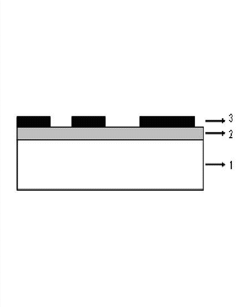
[0023] Aluminum alloy as the base material of the insulating metal substrate is generally selected to have a higher thermal conductivity and a certain mechanical strength, but also can withstand a certain temperature, such as 5052, 6061 and other brands of aluminum. The ceramic used to prepare the insulating layer is aluminum nitride, and the conductive material is copper.

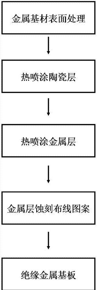
[0024] 1. First use mechanical or chemical methods to remove oil and impurities on the surface of the aluminum plate, and then use the sandblasting process to obtain a clean surface of the workpiece. The thickness of the aluminum plate is 0.5mm;

[0025] 2. Using plasma spraying to grow an aluminum nitride ceramic layer on the surface of the aluminum plate, and controlling the plasma spraying process, the bonding strength of the obtained aluminum nitride coating and the aluminum plate layer is greater than 30MPa, the thickness of the aluminum nitride layer is 0.2mm, and the porosity is low Less than 5%, the r...

Embodiment 2

[0031] Copper alloy is used as the base material for insulating metal substrates, and industrial pure copper with high thermal conductivity is generally selected. The ceramic used to prepare the insulating layer is alumina, and the conductive material is copper-covered silver, mainly to meet the high requirements of high-power package holders for the surface reflectivity of the conductive metal layer;

[0032] 1. First use mechanical or chemical methods to remove oil and impurities on the surface of the copper plate, and then use the sandblasting process to obtain a clean surface of the workpiece. The thickness of the copper plate is 1 mm;

[0033] 2. Using plasma spraying to grow an alumina ceramic layer on the surface of the aluminum plate, and controlling the plasma spraying process, the bond strength of the obtained alumina coating and the aluminum plate layer is greater than 30MPa, the thickness of the alumina layer is 0.4mm, and the porosity is less than 5% , The resistivit...


PUM

PropertyMeasurementUnit
Thicknessaaaaaaaaaa
Thicknessaaaaaaaaaa
Resistivityaaaaaaaaaa

Abstract

The invention discloses a method for manufacturing an insulating metal base plate of an electronic circuit. The method comprises the following steps of: 1. treating the surface of a metal base plate to obtain a clean and smooth surface; 2. depositing a ceramic heat-conduction insulating layer on the surface of a metal plate in a thermal spraying manner; 3. depositing a conductive metal layer on ceramic by utilizing the thermal spraying manner; and 4. etching a wiring pattern on the conductive metal layer of the upper part by utilizing a mask photoetching method. Through the method for manufacturing the insulating metal base plate of the electronic circuit disclosed by the invention, the manufacturing cost of the insulating metal base plate is low, and the manufactured insulating metal base plate has great potential to replace an existing expensive DBC base plate.

Description

Technical field [0001] The invention relates to the field of material preparation technology, in particular to a method for preparing an insulating metal substrate of an electronic circuit. Background technique [0002] With the rapid development of manufacturing technology, the power and volume of electronic products are getting larger and larger, resulting in higher and higher integration. High-power LED is a commonly used electronic device, among which the heating device is mainly a chip, and the heat generated by the chip is mainly exported to the substrate through the package bracket. With the increasing power of a single LED, the heat generation of the chip is also increasing, so higher heat dissipation requirements are also put forward for the LED package bracket. Currently, there are two main types of brackets used in high-power LED packages, which are divided into metal bases and ceramic bases. Ceramic-based stents generally have only two layers, namely the ceramic lay...

Claims


Application Information

Patent Timeline
IPC IPC(8): H05K3/00H05K3/02H05K3/38
Inventor 王春华王一平万军平
Owner 苏州衡业新材料科技有限公司
Why Eureka
Try Eureka