High power LED package

a technology of led package and led light, which is applied in the direction of basic electric elements, electrical equipment, and semiconductor devices, etc., can solve the problems of reducing heat radiation ability, deteriorating light properties of led, and low heat transfer rate, and achieves the effect of increasing heat radiation properties and high power

Inactive Publication Date: 2005-12-15
LG ELECTRONICS INC
View PDF23 Cites 162 Cited by
  • Summary
  • Abstract
  • Description
  • Claims
  • Application Information

AI Technical Summary

Benefits of technology

[0014] Accordingly, the present invention has been made keeping in mind the above problems occurring in the related art, and an object of the present invention is to provide a high power LED package for use in backlight

Problems solved by technology

In the above LED package, heat generated upon operation of the LED is not directly transferred to the aluminum heat sink 211 manifesting excellent heat radiation ability, but is transferred thereto through the plastic body 205 and the PCB 210, both of which have a low heat transfer rate, thus reducing heat radiation ability, resulti

Method used


Image

  • High power LED package
  • High power LED package
  • High power LED package

Examples


first embodiment

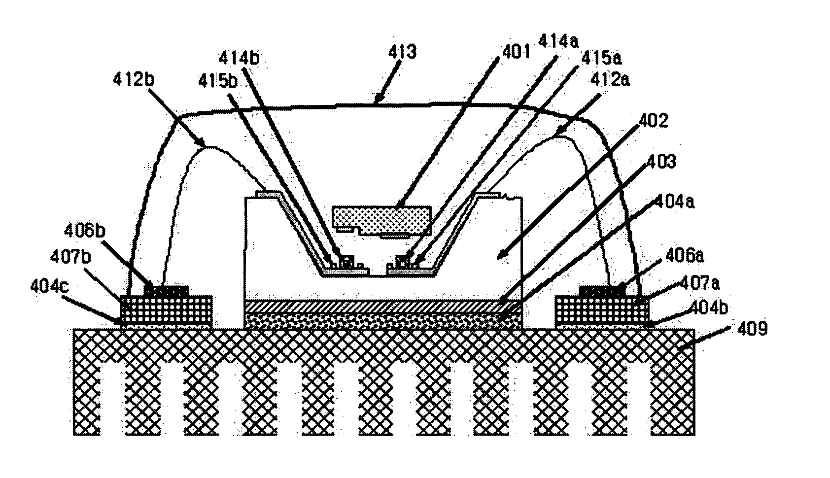
[0032]FIG. 3 is a sectional view showing the high power LED package, according to the present invention.

[0033] According to the first embodiment, the high power LED package includes an LED 401, a silicon submount 402, an insulating layer 403, an adhesive 404a, metal lines 406a and 406b, insulating substrates 407a and 407b, a heat sink 409, electrical wires 412b and 412b, a lens 413, solders 414a and 414b, and solder dams 415b and 415b.

[0034] In the high power LED package, the silicon submount 402 having the LED 401 flip chip bonded thereto is directly attached to the upper surface of the heat sink 409 using the adhesive 404a. As such, the adhesive 404a includes a material having excellent heat conductivity and a heat expansion coefficient similar to that of the submount 402, and is exemplified by an aluminum paste, and a silver paste. Further, the heat sink 409 may be formed of a conductor or a nonconductor.

[0035] Referring to FIG. 3, the silicon submount 402 has a groove to recei...

second embodiment

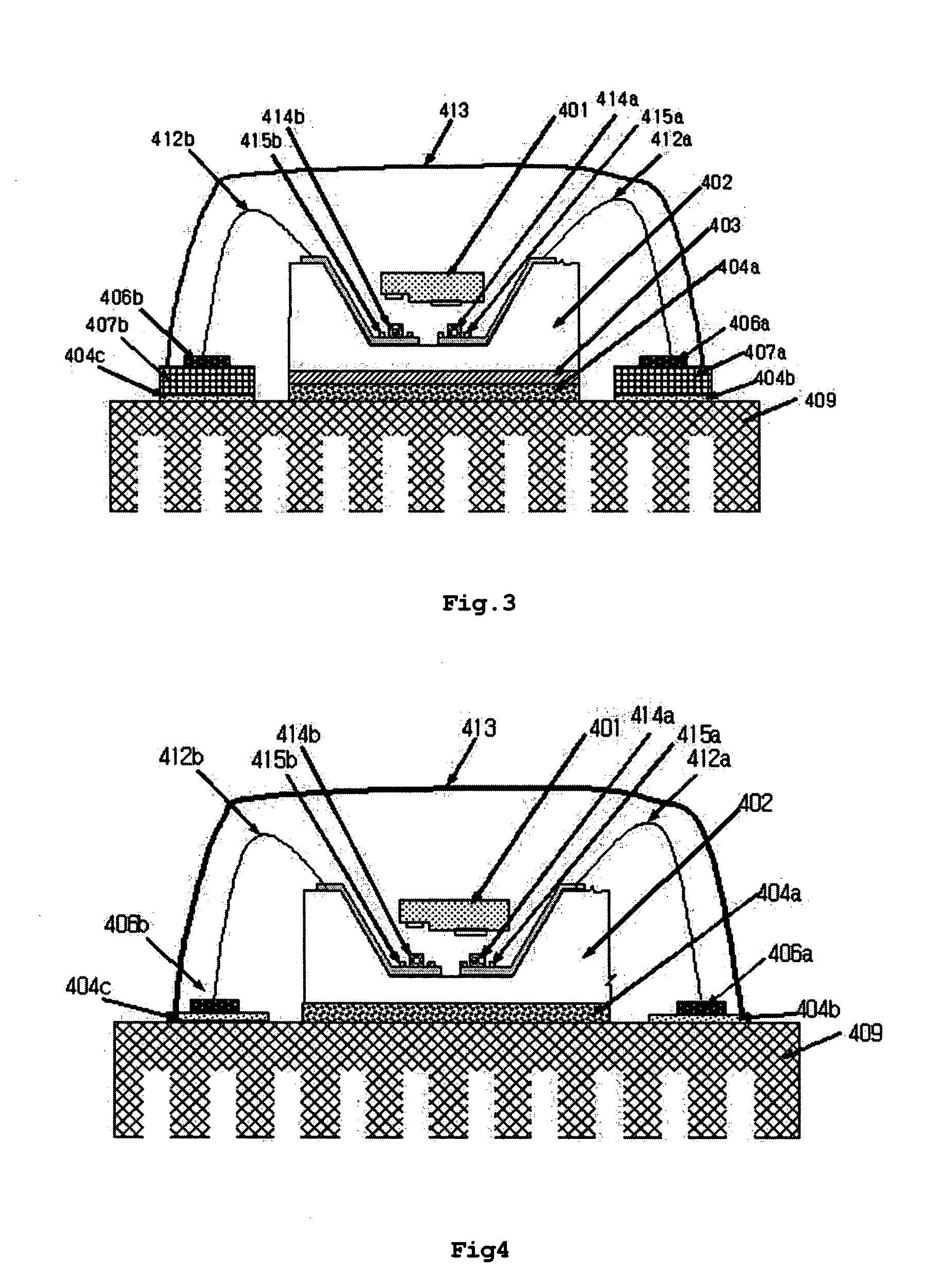
[0042]FIG. 4 is a sectional view showing the high power LED package, according to the present invention. In the above LED package, a silicon submount 402 having an LED 401 flip chip bonded thereto is directly attached to the upper surface of a heat sink 409 composed of a nonconductor including an insulating film formed of AlN, AlOx, etc. Also, the LED 401 is electrically connected to the exterior via a predetermined metal line, which includes conductive metal lines 406a and 406b provided on the insulating substrates 407a and 407b of the PCB as in the LED package shown in FIG. 3, or conductive metal lines 406a and 406b directly attached to the upper surface of the heat sink 409 without insulating substrates 407a and 407b.

[0043] Adhesives 404a, 404b and 404c, wires 412b and 412b, and a lens 413 remain the same as in the first embodiment of the present invention shown in FIG. 3.

[0044] Turning now to FIG. 5, a perspective view showing the LED package in an array configuration, accordi...


PUM


Abstract

Disclosed is a high power LED package, including an LED; a silicon submount to which the LED is flip chip bonded; a reflective film formed on the silicon submount and electrically connected to the LED to increase light emitting efficiency of the LED; electrical wires connected to the reflective film to connect the LED to an external circuit; an insulating body formed below the silicon submount; a heat sink formed below the insulating body; an insulating substrate formed on the heat sink; and metal lines formed on the insulating substrate and connected to the electrical wires. In the LED package, since the silicon submount having the LED flip chip bonded thereto is directly attached to the heat sink, heat generated upon operation of the LED can be effectively radiated. Also, the LED package has a simple structure, thus having drastically decreased manufacturing costs. The high power LED can be applied to backlight units of LCDs or general illumination fixtures, and as well, to backlight units of conventional PCS phones or LED packages for key pads, therefore increasing the light properties of the LED. In particular, the LED package has an array of two or more submounts each having an LED flip chip bonded thereto, and thus, it can be applied to a module of a backlight unit for LCDs, thus having remarkably reduced manufacturing costs.

Description

BACKGROUND OF THE INVENTION [0001] 1. Field of the Invention [0002] The present invention relates, generally, to a high power LED package, and, more particularly, to a package structure that efficiently radiates heat generated upon operation of the LED. [0003] 2. Description of the Related Art [0004] An LED (Light Emitting Diode), which is advantageous because it manifests energy saving effects superior to conventional light sources and may be semi-permanently used, is receiving attention as a next-generation light source in an era of light semiconductors leading compound semiconductors into the 21st century. Recently, because luminance problems of LEDs have been drastically improved, the LED is variously applied in all industrial fields, including backlight units, automobiles, electric signs, traffic signal lamps, illumination fixtures, etc. [0005] In particular, an LED having a small size and high luminance for use in backlight units has been substituted for a CCFL lamp serving as...

Claims


Application Information

Patent Timeline
IPC IPC(8): H01L33/46H01L33/58H01L33/60H01L33/62H01L33/64
CPCH01L33/62H01L33/642H01L2224/48091H01L2224/73265H01L2924/00014H01L2924/3011H01L2924/00H01L2924/10253
Inventor KIM, GEUN-HOPARK, CHIL-KEUNSONG, KI-CHANG
Owner LG ELECTRONICS INC
Why Eureka
Try Eureka