Semiconductor element bonding substrate, semiconductor device, and power conversion device

a technology of semiconductor devices and semiconductor elements, applied in semiconductor devices, semiconductor/solid-state device details, electrical apparatus, etc., can solve the problems of reduced characteristics and easy shrinkage of the shell cavity, and achieve the effects of reducing the shrinkage of the fillet part, improving heat radiation properties, and increasing heat capacity

Active Publication Date: 2020-04-30
MITSUBISHI ELECTRIC CORP
View PDF0 Cites 3 Cited by
  • Summary
  • Abstract
  • Description
  • Claims
  • Application Information

AI Technical Summary

Benefits of technology

[0010]In the semiconductor element bonding substrate according to the present invention, the concave part is provided near the edge of the bonding region in the main surface of the metal pattern. The solder is supplied to an inner side of the concave part when the semiconductor element is solder-bonded to the bonding region. When the melted solder is clotted, the solder filling the inner side of the concave part shrinks, thereby reducing a shrinkage of a fillet part of the solder. Thus, it can be suppressed that a shrinkage cavity occurs in the fillet part of the solder and the shrinkage cavity enters a lower side of the semiconductor element. The occurrence of the shrinkage cavity in the solder is suppressed, thus the heat radiation property can be improved in the semiconductor device.
[0011]According to the semiconductor element bonding substrate in the present embodiment, the height of the main surface of the metal pattern is made different between the center part of the bonding region and the surrounding area of the center part, thus a timing of clotting the solder can be made different between the center part of the bonding region and the surrounding area of the center part. For example, the height of the center part of the bonding region 6a is lowered than the surrounding area of the center part, thus the solder is supplied to the depressed part in a center of the bonding region, and the solder filling the depressed part increases a heat capacity in a portion immediately below the center part of the semiconductor element. Accordingly, the solder located near the edge of the bonding region can be clotted first. That is to say, the center part of the bonding region is a part where the solder is clotted last, thus an occurrence of a shrinkage cavity can be suppressed in a fillet part where the solder is clotted early. The center part of the bonding region has the height higher than the surrounding area of the center part, a larger amount of solder is supplied to the surrounding area of the center part of the bonding region compared to the center part. Thus, when the melted solder is clotted, the solder in the surrounding area of the center part of the bonding region shrinks, thereby reducing a shrinkage of a fillet part of the solder. Thus, an occurrence of a shrinkage cavity can be suppressed in a fillet part of the solder. The occurrence of the shrinkage cavity in the solder is suppressed, thus the heat radiation property can be improved in the semiconductor device.
[0012]These and other objects, features, aspects and advantages of the present invention will become more apparent from the following detailed description of the present invention when taken in conjunction with the accompanying drawings.

Problems solved by technology

These types of solders have a problem that a solder shrinkage cavity easily occurs.
However, when a solder shrinkage cavity occurs immediately below the semiconductor element, a heat radiation property at a time of an occurrence of heat in the semiconductor element is reduced, and it leads to a reduction in characteristics.

Method used


Image

  • Semiconductor element bonding substrate, semiconductor device, and power conversion device
  • Semiconductor element bonding substrate, semiconductor device, and power conversion device
  • Semiconductor element bonding substrate, semiconductor device, and power conversion device

Examples


embodiment 1

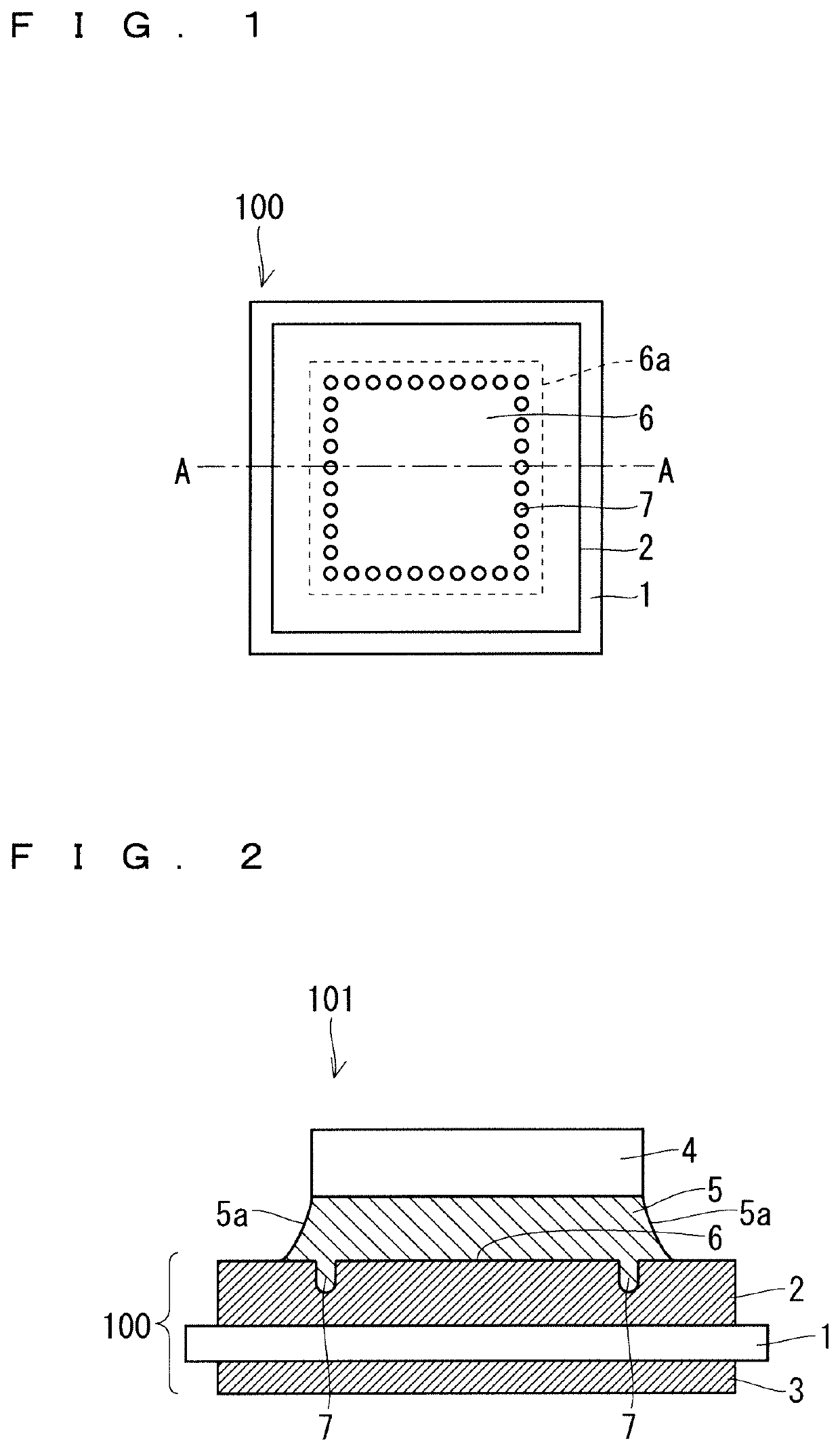
[0028]FIG. 1 is a plan view of a semiconductor element bonding substrate 100 according to a present embodiment 1. FIG. 2 is a cross-sectional view of a semiconductor device 101 according to the present embodiment 1. In the semiconductor device 101 illustrated in FIG. 2, a semiconductor element 4 is bonded to a bonding region 6a in the semiconductor element bonding substrate 100 by a solder 5. A cross section of the semiconductor device 101 illustrated in FIG. 2 corresponds to a cross section along a line segment A-A in FIG. 1.

[0029]The semiconductor element bonding substrate 100 includes an insulating plate 1 and a metal pattern 2. The metal pattern 2 is bonded to a main surface of the insulating plate 1. A main surface 6 of the metal pattern 2 on an opposite side of the insulating plate 1 includes the bonding region 6a to which the semiconductor element 4 is bonded by the solder 5. A plurality of concave parts 7 are formed in the bonding region 6a in the main surface 6 of the metal...

embodiment 2

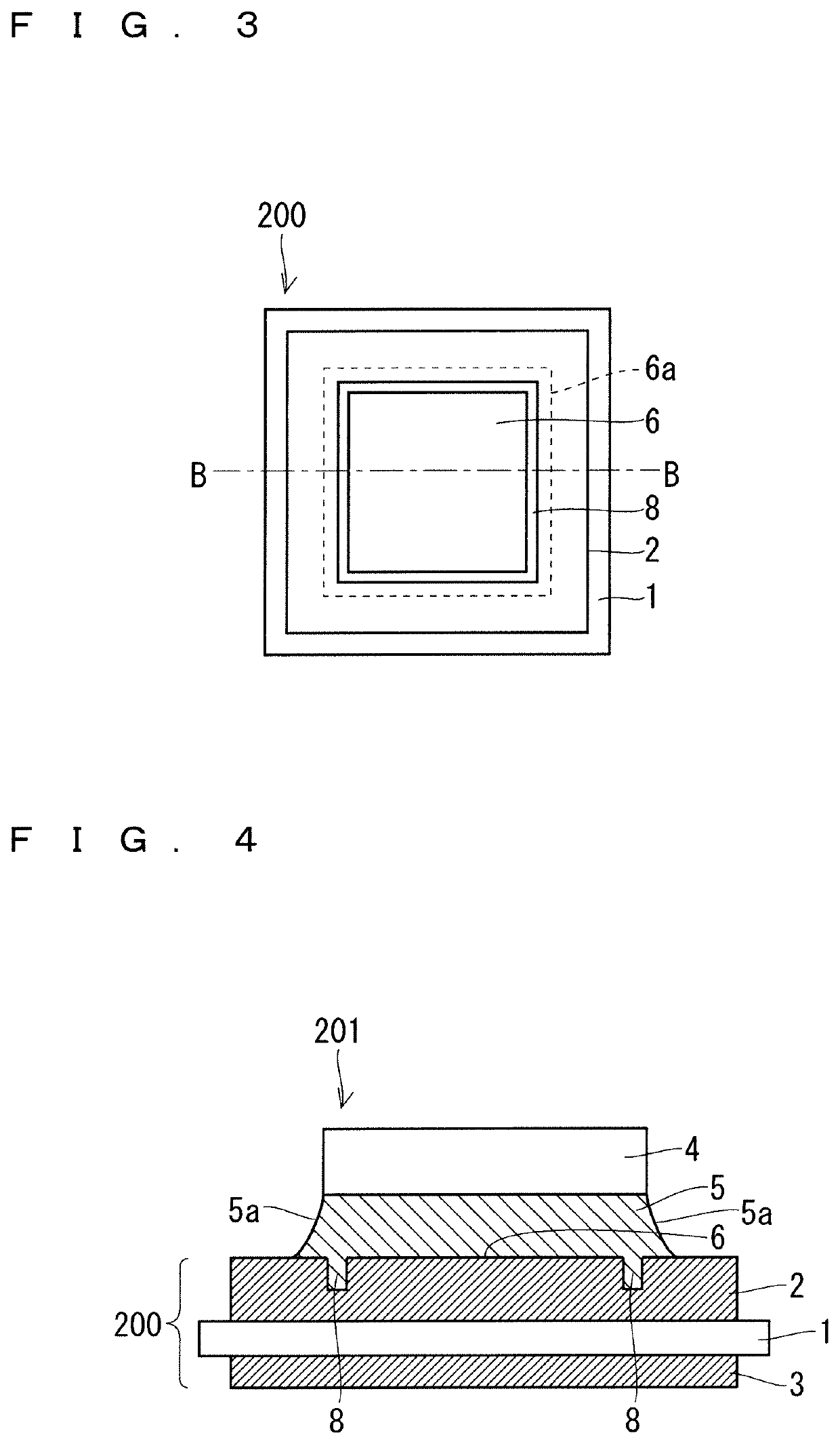
[0037]FIG. 3 is a plan view of a semiconductor element bonding substrate 200 according to a present embodiment 2. FIG. 4 is a cross-sectional view of a semiconductor device 201 according to the present embodiment 2. In the semiconductor device 201 illustrated in FIG. 4, a semiconductor element 4 is bonded to a bonding region 6a in the semiconductor element bonding substrate 200 by a solder 5. A cross section of the semiconductor device 201 illustrated in FIG. 4 corresponds to a cross section along a line segment B-B in FIG. 3.

[0038]The semiconductor element bonding substrate 200 includes an insulating plate 1 and a metal pattern 2. The metal pattern 2 is bonded to a main surface of the insulating plate 1. A main surface 6 of the metal pattern 2 on an opposite side of the insulating plate 1 includes the bonding region 6a to which the semiconductor element 4 is bonded by the solder 5. A continuous groove 8 is formed in the bonding region 6a in the main surface of the metal pattern 2. ...

embodiment 3

[0042]FIG. 5 is a plan view of a semiconductor element bonding substrate 300 according to a present embodiment 3. FIG. 6 is a cross-sectional view of a semiconductor device 301 according to the present embodiment 3. In the semiconductor device 301 illustrated in FIG. 6, a semiconductor element 4 is bonded to a bonding region 6a in the semiconductor element bonding substrate 300 by a solder 5. A cross section of the semiconductor device 301 illustrated in FIG. 6 corresponds to a cross section along a line segment C-C in FIG. 5.

[0043]The semiconductor element bonding substrate 300 further includes a metal member 9 located in each of the plurality of concave parts 7 when compared with the semiconductor element bonding substrate 100 (FIG. 1) in the embodiment 1. The metal member 9 is formed of a material having a larger heat conductivity than the solder 5. The metal member 9 has a spherical shape. The metal member 9 is made of Cu, Ni, Au, Ag, Cu plated with Ni, or Al plated with Ni, for...


PUM

PropertyMeasurementUnit
semiconductoraaaaaaaaaa
heat conductivityaaaaaaaaaa
electrical poweraaaaaaaaaa

Abstract

A semiconductor element bonding substrate according to the present invention includes an insulating plate, and a metal pattern bonded to a main surface of the insulating plate. A main surface of the metal pattern on an opposite side of the insulating plate includes a bonding region to which a semiconductor element is bonded by a solder. The metal pattern includes at least one concave part located in the main surface. The at least one concave part is located closer to an edge of the bonding region in relation to a center part of the bonding region in the bonding region.

Description

TECHNICAL FIELD[0001]The present invention relates to a semiconductor element bonding substrate, a semiconductor device, and a power conversion device.BACKGROUND ART[0002]As a solder for bonding a semiconductor element and an insulating substrate, a non-eutectic solder, which is mainly made of an Sn—Cu based, Sn—Ag based, Sn—Sb based,[0003]Sn-In based, or Sn—Bi based component, is used to secure high reliability. These types of solders have a problem that a solder shrinkage cavity easily occurs.[0004]Recently, a semiconductor element operating under high temperature is intensively developed, and a downsizing, high tolerance, and high current density growth of the semiconductor element are promoted. Particularly, a wideband gap semiconductor such as SiC and GaN has a larger bandgap than an Si semiconductor, thus a high tolerance, downsizing, high current density growth, and operation under high temperature of a semiconductor device are expected (refer to Patent Document 1, for exampl...

Claims


Application Information

Patent Timeline
Patent Type & Authority Applications(United States)
IPC IPC(8): H01L23/00H01L21/52H01L23/13
CPCH01L2224/32225H01L24/32H01L21/52H01L2924/13055H01L23/13H01L2224/83385H01L23/12H01L2924/15159H01L23/3735H01L2224/26152H01L2224/26155H01L2224/26175H01L2924/13091H01L2924/10272H01L2224/83455H01L2924/1033H01L24/83H01L24/29
Inventor ISHIKAWA, SATORU
Owner MITSUBISHI ELECTRIC CORP
Why Eureka
Try Eureka