Semiconductor device

a technology of semiconductor devices and semiconductor substrates, applied in semiconductor devices, semiconductor/solid-state device details, electrical apparatus, etc., can solve the problems of poor wiring layout efficiency, inability to make small wiring substrates, and extremely narrow space between respective bump lands, so as to shorten the wiring route from through holes to external terminals, the effect of miniaturizing the semiconductor devi

Inactive Publication Date: 2006-07-06
RENESAS ELECTRONICS CORP
View PDF1 Cites 8 Cited by
  • Summary
  • Abstract
  • Description
  • Claims
  • Application Information

AI Technical Summary

Benefits of technology

[0022] Since a plurality of through holes of the wiring substrate are formed by laser beam machining, an opening of the through hole can be made small. Thereby, since an external terminal can be arranged directly under the through hole in a semiconductor device, a wiring substrate can be made small and, as a result, miniaturization of the semiconductor device can be achieved. Since it becomes possible to arrange the through hole and the land connecting the external terminal in the same location, the wiring route from the through hole to an external terminal can be shortened, and improvement in the heat radiation property of the semiconductor device can be achieved.

Problems solved by technology

When a bump land and a through hole are arranged in the limited wiring area, the space between respective bump lands becomes extremely narrow.
Even if it is the case where there is no restriction in a layout space, the efficiency of a wiring layout is bad and a wiring substrate cannot be made small.
Thereby, it poses a problem that a narrowed pitch, increased pin count, and miniaturization of a semiconductor device cannot be realized.

Method used


Image

  • Semiconductor device
  • Semiconductor device
  • Semiconductor device

Examples


embodiment 1

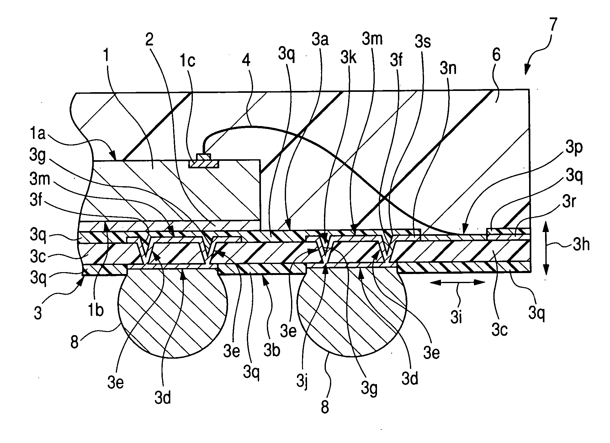
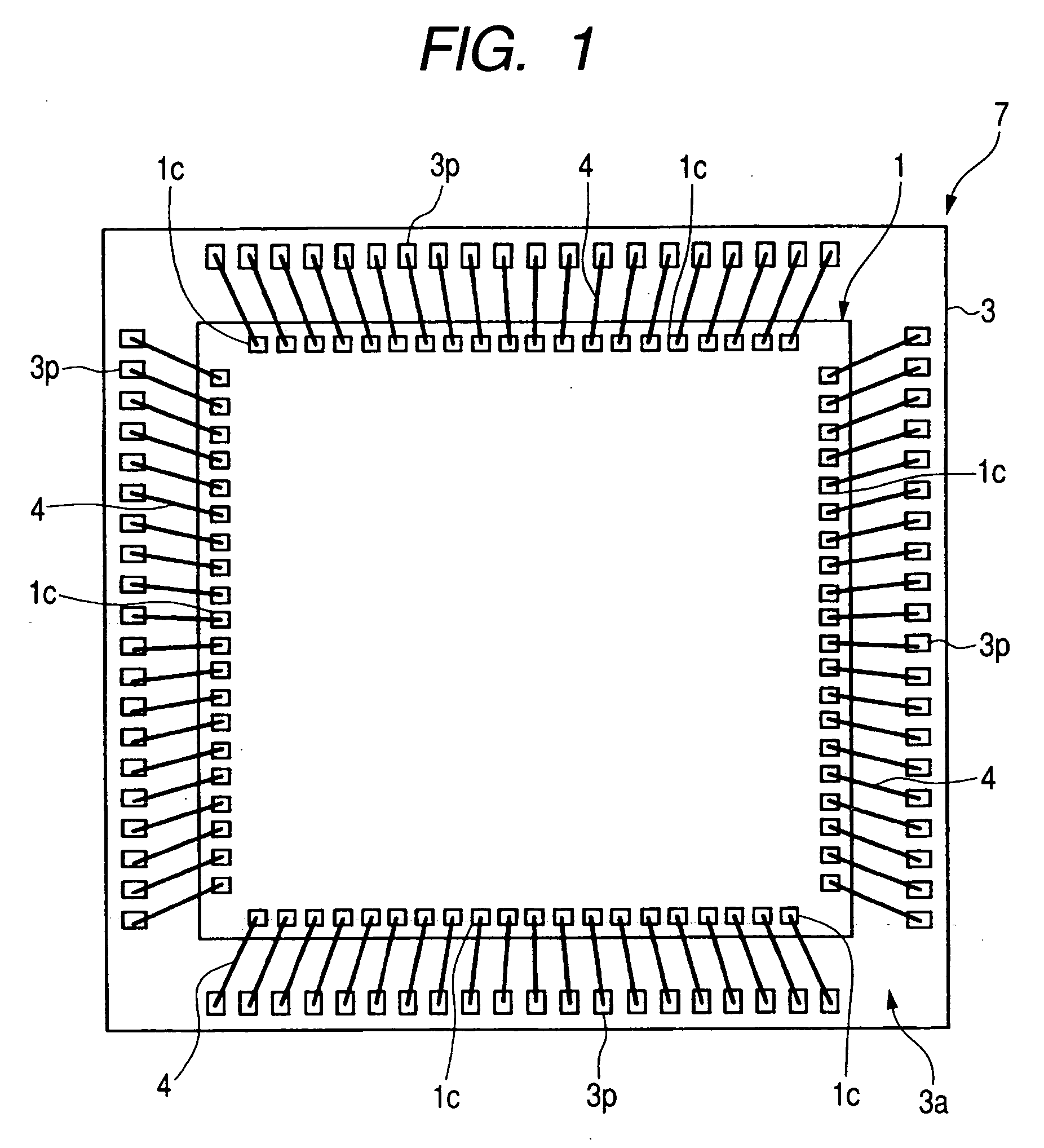
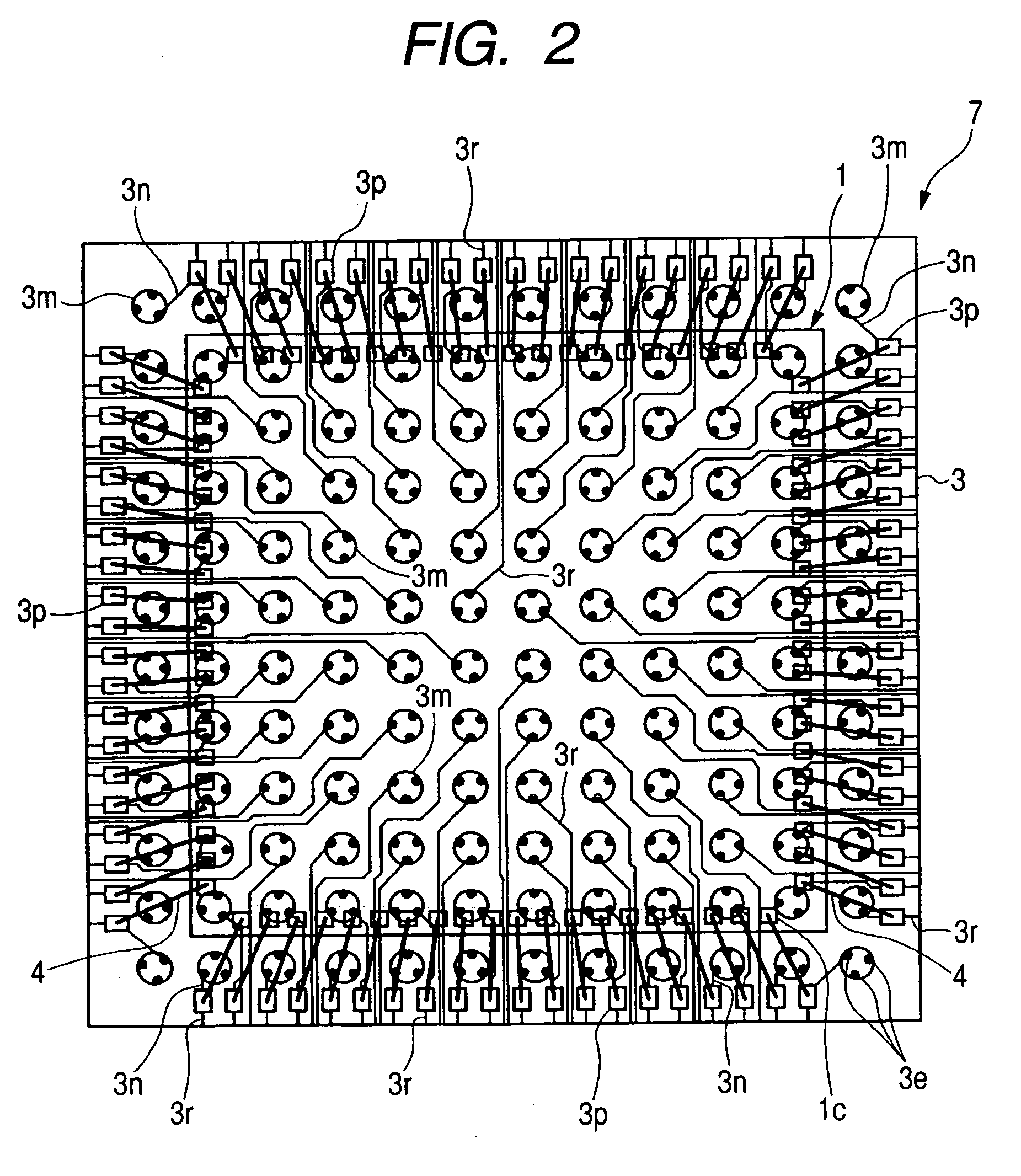
[0063]FIG. 1 is a plan view showing an example of the structure of the semiconductor device of Embodiment 1 of the present invention, FIG. 2 is a plan view showing an example of the conductor pattern on the main surface side of a wiring substrate penetrating a molded body and a semiconductor chip in the semiconductor device shown in FIG. 1, FIG. 3 is a sectional view showing an example of the structure of the semiconductor device shown in FIG. 1, FIG. 4 is an enlarged partial sectional view showing the structure of the section A shown in FIG. 3; FIG. 5 is a plan view showing an example of the structure of the wiring substrate included in the semiconductor device shown in FIG. 1; FIG. 6 is a sectional view showing an example of the structure of the wiring substrate shown in FIG. 5, FIG. 7 is an enlarged partial sectional view showing the structure of the section A shown in FIG. 6, FIG. 8 is a manufacturing process flow chart showing an example of the assembly up to a resin molding in...

embodiment 2

[0112]FIG. 21 is a plan view showing an example of the conductor pattern on the main surface side of a wiring substrate penetrating a molded body and a semiconductor chip in the semiconductor device of Embodiment 2 of the present invention; FIG. 22 is a sectional view showing an example of the structure of the semiconductor device shown in FIG. 21, FIG. 23 is an enlarged partial sectional view showing the structure of the section A shown in FIG. 22, FIG. 24 is a plan view showing an example of the structure of the wiring substrate included in the semiconductor device shown in FIG. 21, FIG. 25 is a sectional view showing an example of the structure of the wiring substrate shown in FIG. 24, FIG. 26 is an enlarged partial sectional view showing the structure of the section A shown in FIG. 25, FIG. 27 is a plan view showing the conductor pattern on the main surface side of a wiring substrate penetrating a molded body and a semiconductor chip in the semiconductor device of the modificati...

embodiment 3

[0121]FIG. 30 is a plan view showing an example of the conductor pattern on the main surface side of a wiring substrate penetrating a molded body and a semiconductor chip in the semiconductor device of Embodiment 3 of the present invention, FIG. 31 is a sectional view showing an example of the structure of the semiconductor device shown in FIG. 30, FIG. 32 is an enlarged partial sectional view showing the structure of the section A shown in FIG. 31, FIG. 33 is a plan view showing an example of the structure of the wiring substrate included in the semiconductor device shown in FIG. 30, FIG. 34 is a sectional view showing an example of the structure of the wiring substrate shown in FIG. 33, FIG. 35 is an enlarged partial sectional view showing the structure of the section A shown in FIG. 34, and FIG. 36 is a plan view showing the conductor pattern on the main surface side of the wiring substrate of the modification of Embodiment 3 of the present invention.

[0122] The semiconductor dev...


PUM


Abstract

The miniaturization of a semiconductor device is aimed at. A package substrate have a plurality of terminals formed on the main surface, a plurality of lands formed on the back surface, through holes which are formed by laser beam machining and have been arranged at the upper part of each of the plurality of lands, and plating films which are arranged in the through hole and connect the land with the terminal electrically, a semiconductor chip which is mounted on the main surface of the package substrate, a conductive wire which connects the pad of the semiconductor chip and the package substrate, and a plurality of solder bumps formed in the lands of the package substrate. Since the through hole is formed by laser beam machining, the opening of the through hole is small. It becomes possible to arrange a solder bump directly under the through hole, and miniaturization of CSP 7 (semiconductor device) can be realized.

Description

CROSS-REFERENCE TO RELATED APPLICATION [0001] The present application claims priority from Japanese patent application No. 2005-000735 filed on Jan. 5, 2005, the content of which is hereby incorporated by reference into this application. FIELD OF THE INVENTION [0002] The present invention relates to a semiconductor device, and particularly relates to an effective technology in the application to narrow a pitch, increase pin count, and miniaturize a semiconductor device. DESCRIPTION OF THE BACKGROUND ART [0003] In a semiconductor device such as of a BGA (Ball Grid Array) type and a CSP (Chip Size Package) type, a die pattern smaller than the IC chip size and solder resist larger than the IC chip size and extending over the whole surface of a wiring board are formed on an IC chip adhesion side of the wiring board. A metallic pattern and solder resist having almost the same areas as in the IC chip adhesion side are formed on the side opposite to the IC chip adhesion side of the wiring ...

Claims


Application Information

Patent Timeline
Patent Type & Authority Applications(United States)
IPC IPC(8): H01L23/04
CPCH01L23/49816H01L23/49827H01L23/49838H01L24/45H01L24/97H01L2224/45144H01L2224/48091H01L2224/49171H01L2224/73265H01L2224/97H01L2924/01004H01L2924/01014H01L2924/01029H01L2924/01078H01L2924/01079H01L2924/14H01L2924/15311H01L2924/00014H01L2224/85H01L2224/83H01L2224/92247H01L24/48H01L2224/32225H01L2224/48227H01L2924/01006H01L2924/01033H01L24/49H01L2924/00H01L2924/01028H01L2924/00012H01L24/73H01L2224/05554H01L2224/49433H01L2924/181
Inventor SHIMANUKI, YOSHIHIKO
Owner RENESAS ELECTRONICS CORP
Why Eureka
Try Eureka