Semiconductor device and method for manufacturing the same

Inactive Publication Date: 2004-04-29
PANASONIC CORP
View PDF0 Cites 1 Cited by
  • Summary
  • Abstract
  • Description
  • Claims
  • Application Information

AI Technical Summary

Benefits of technology

0016] In view of these problems in the prior art, a first object of the present invention is to provide a semiconductor device using a group III-V nitride semiconductor, in which a current constriction section can

Problems solved by technology

The crystal growth of a group III-V nitride semiconductor, or a so-called "gallium nitride (GaN) semiconductor", has been difficult, as is also the case with other wide gap semiconductors.
Moreover, since a substrate made of gallium nitride is difficult to produce, a gallium nitride semiconductor cannot be grown by a crystal growth technique that is used with silicon (Si) or gallium arsenide (GaAs), i.e., growing a semiconductor layer (epitaxial growth layer) on a substrate having the same composition as that of the semiconductor layer.
Moreover, since it is typically difficult to perform a wet etching process with an acidic solution, or the like, on a nitride semiconductor, a dry etching method such as reactive ion etching i

Method used


Image

  • Semiconductor device and method for manufacturing the same
  • Semiconductor device and method for manufacturing the same
  • Semiconductor device and method for manufacturing the same

Examples


first embodiment

SECOND VARIATION OF FIRST EMBODIMENT

[0137] A second variation of the first embodiment of the present invention will now be described with reference to the drawings.

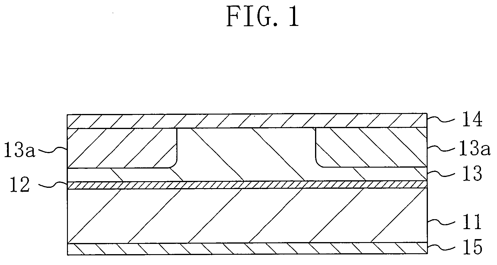
[0138] FIG. 5 is a cross-sectional view illustrating a semiconductor device according to the second variation of the first embodiment of the present invention. In FIG. 5, those components that are already shown in FIG. 1 are denoted by the same reference numerals, and will not be further described below.

[0139] As illustrated in FIG. 5, oxidized regions 13b of the semiconductor device of the second variation are formed so as to include the light emitting layer 12 and an upper portion of the n-type first semiconductor layer 11. Thus, the externally injected current can be constricted more reliably, thereby further reducing the leakage current in the light emitting layer 12.

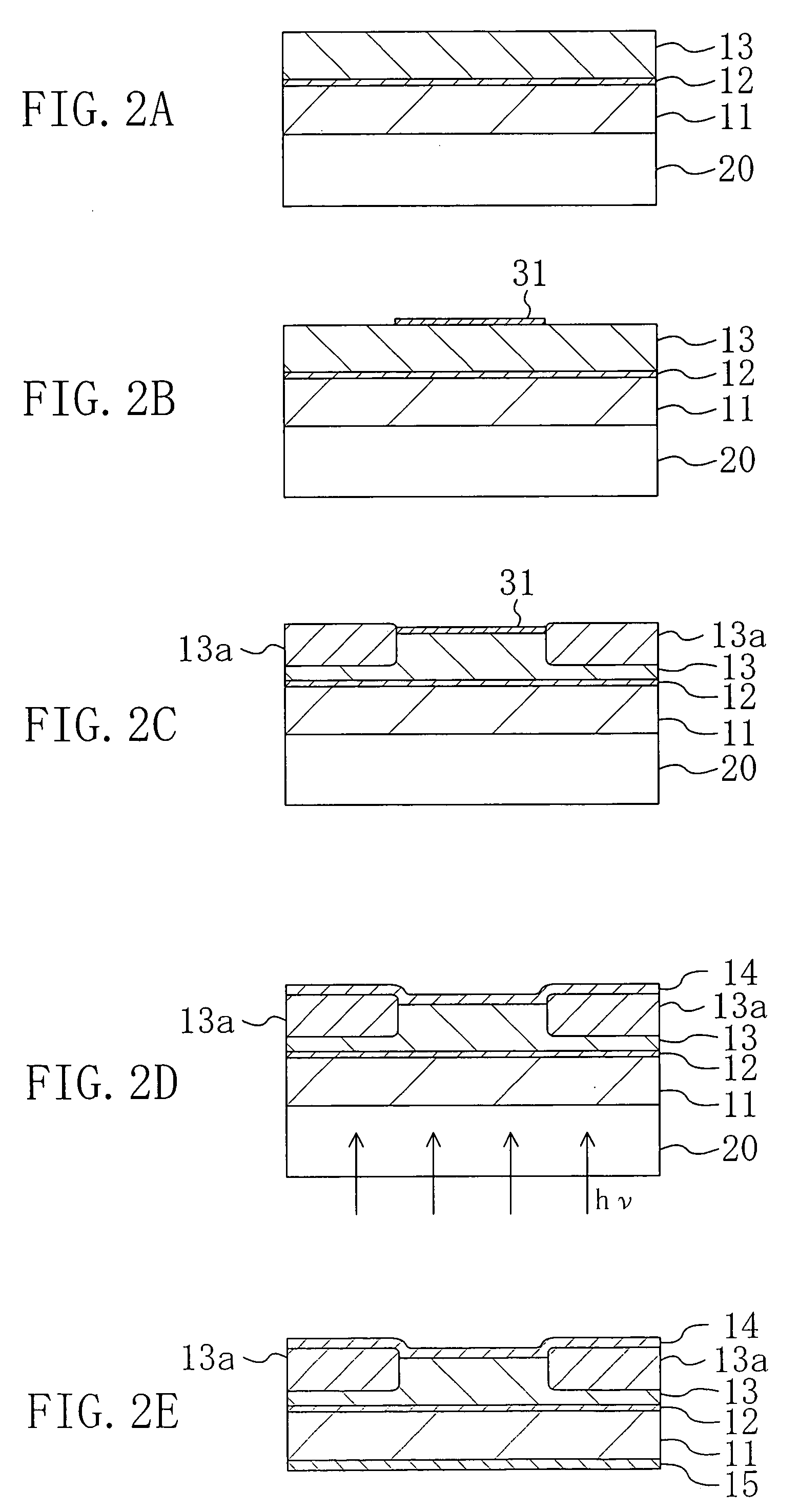
[0140] With the first manufacturing method, the oxidized regions 13b can be formed by growing the structure up to the second semiconductor layer 13, and ...

second embodiment

[0144] The second embodiment of the present invention will now be described with reference to the drawings.

[0145] FIG. 6 is a cross-sectional view illustrating, as a semiconductor device according to the second embodiment of the present invention, a semiconductor light emitting device that can be applied to a light emitting diode device or a semiconductor laser device. In FIG. 6, those components that are already shown in FIG. 1 are denoted by the same reference numerals, and will not be further described below.

[0146] In the semiconductor device of the second embodiment, a substrate 21 made of p-type silicon carbide (SiC) oriented along the (0001) plane, for example, is provided on one surface of the p-type second semiconductor layer 13 that is away from the light emitting layer 12.

[0147] Moreover, a p-side electrode 17 as the first ohmic electrode made of an alloy of aluminum (Al) and silicon (Si), e.g., an Al--Si alloy (Al: 89%), is formed on one surface of the substrate 21 that i...

third embodiment

[0165] The third embodiment of the present invention will now be described with reference to the drawings.

[0166] FIG. 8 is a cross-sectional view illustrating, as a semiconductor device according to the third embodiment of the present invention, a semiconductor light emitting device that can be applied to a light emitting diode device or a semiconductor laser device. In FIG. 8, those components that are already shown in FIG. 1 are denoted by the same reference numerals, and will not be further described below.

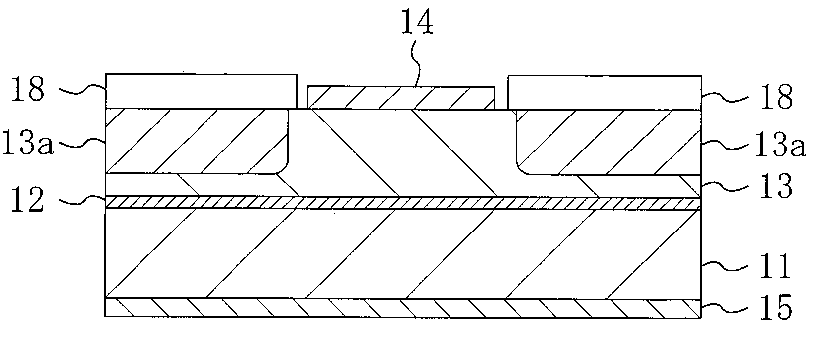
[0167] The semiconductor device of the third embodiment is characterized in that the exposed surfaces of the oxidized regions 13a, which form the current constriction section, are covered by an insulating film 18 made of silicon oxide (SiO.sub.2). Moreover, the p-side electrode 14 is selectively formed on a region of the second semiconductor layer 13 between the oxidized regions 13a.

[0168] Thus, as in the first embodiment, the semiconductor device of the third embodiment does n...


PUM


Abstract

A light emitting layer made of a group III-V nitride semiconductor is formed between a first semiconductor layer made of an n-type group III-V nitride semiconductor and a second semiconductor layer made of a p-type group III-V nitride semiconductor. In side portions of the second semiconductor layer, oxidized regions are formed through the oxidization of the second semiconductor layer itself so as to be spaced apart from each other in the direction parallel to the plane of the light emitting layer. A p-side electrode is formed across the entire upper surface of the second semiconductor layer including the oxidized regions, and an n-side electrode is formed on one surface of the first semiconductor layer that is away from the second semiconductor layer.

Description

BACKGROUND OF THE INVENTION[0001] The present invention relates to a semiconductor device such as a short-wavelength light emitting diode device or a short-wavelength semiconductor laser device, and a method for manufacturing the same.[0002] A semiconductor material made of a group III-V nitride semiconductor, having a wide forbidden band, can be used in light emitting devices, specifically, light emitting diode devices and short-wavelength semiconductor laser devices that are capable of emitting light of a color in a visible region such as blue, green or white. Among others, light emitting diode devices have already been in practical use in large-size display apparatuses, traffic signals, etc. Particularly, white light emitting diode devices, which give white light by exciting a fluorescent substance, are expected to replace conventional lighting fixtures such as electric bulbs and fluorescent lamps. Moreover, the development of semiconductor laser devices has reached a point where...

Claims


Application Information

Patent Timeline
IPC IPC(8): H01L21/00H01L21/20H01L21/76H01L27/01H01L33/06H01L33/32H01L33/36H01L33/44H01S5/02H01S5/024H01S5/042H01S5/22H01S5/223H01S5/227H01S5/323H01S5/343
CPCH01S2304/12H01S5/227H01S5/0215H01L21/0262H01S5/2232H01S2304/04H01S5/32341H01S5/2215H01L21/02639H01L21/02532H01L21/0237H01S5/0425H01S5/2231H01S5/0213H01L21/7605H01S5/2214H01L21/0254H01S5/0217H01L33/145H01S2301/176H01S5/04254H01S5/04257
Inventor UEDA, TETSUZO
Owner PANASONIC CORP
Why Eureka
Try Eureka