Flat panel display device and method of fabricating the same

a flat panel display and display device technology, applied in non-linear optics, identification means, instruments, etc., can solve problems such as image quality degradation and signal delay in signal wiring in flat panel displays, and achieve the effects of low wiring resistance, thermal stability, and improved contact resistan

Active Publication Date: 2007-11-13
SAMSUNG DISPLAY CO LTD
View PDF22 Cites 13 Cited by
  • Summary
  • Abstract
  • Description
  • Claims
  • Application Information

AI Technical Summary

Benefits of technology

[0010]The present invention provides a flat panel display device including a source / drain electrode having low wiring resistance, thermal stability and improved contact resistance with the pixel electrode.

Problems solved by technology

This means that it may increase wiring resistance of the signal wiring, creating a signal delay in the signal wiring.
The signal delay may cause image quality degradation in a flat panel display.

Method used


Image

  • Flat panel display device and method of fabricating the same
  • Flat panel display device and method of fabricating the same
  • Flat panel display device and method of fabricating the same

Examples


Embodiment Construction

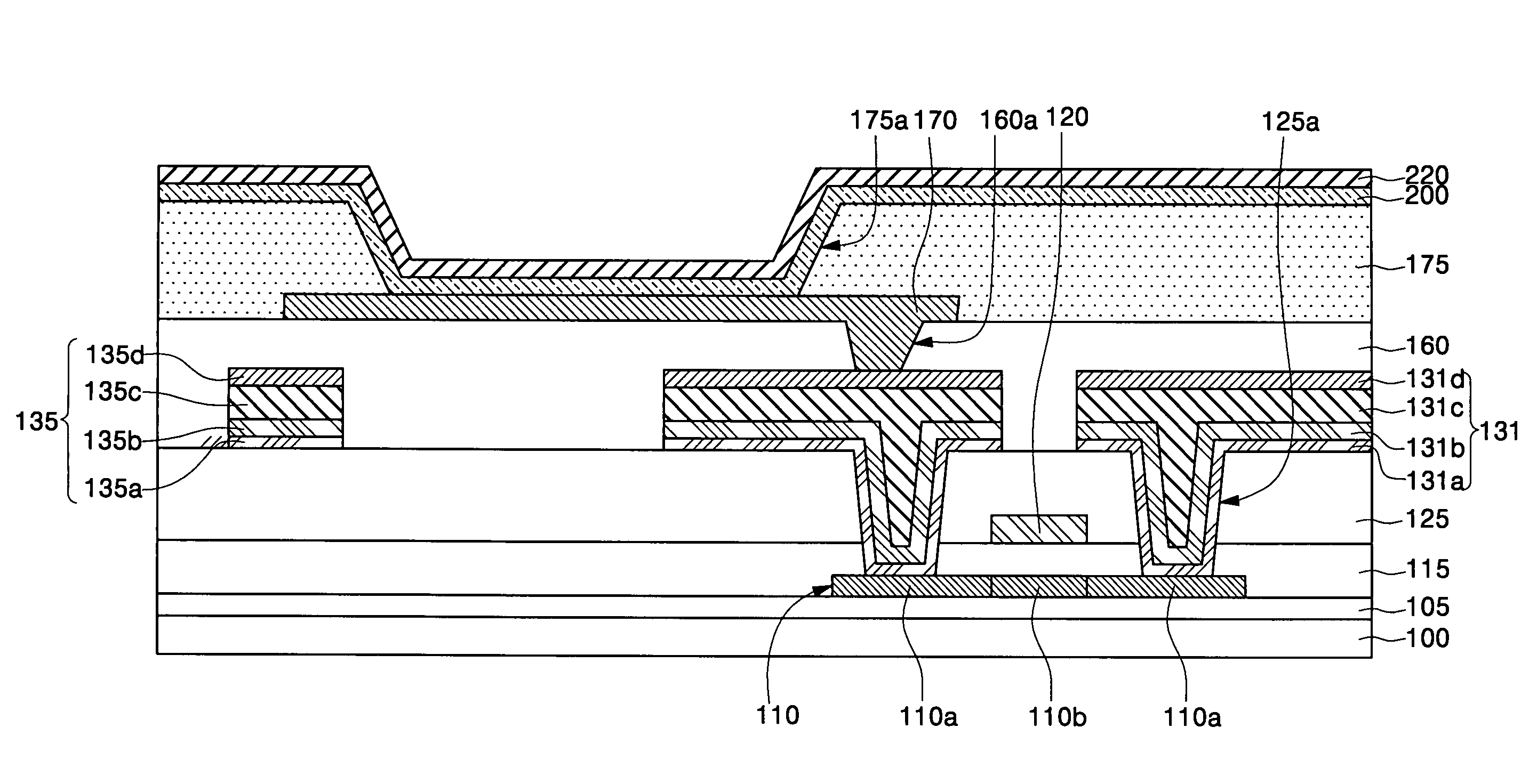
[0024]The present invention will now be described more fully with reference to the accompanying drawings, in which preferred embodiments of the invention are shown. This invention may, however, be embodied in different forms and should not be construed as limited to the embodiments set forth herein. In the drawings, when one layer is shown as located “on” another layer or a substrate, one should understand that this means that one layer can be directly formed on the other layer of the substrate or another (third or more) layer can be interposed between these layers. Like numbers refer to like elements throughout the specification.

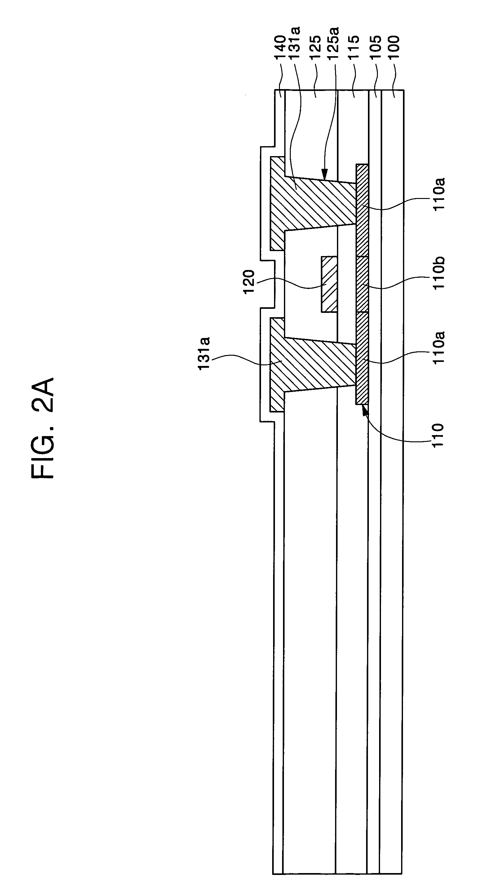
[0025]As shown in FIG. 2A, a substrate 100 may be provided. The substrate 100 can be a glass or plastic substrate. A buffer layer 105 may be formed on the substrate 100. The buffer layer 105 can be formed of a silicon oxide layer, a silicon nitride layer, silicon oxynitride layer, a similar layer, or a multiple layers thereof. The buffer layer 105 may be a ...


PUM

PropertyMeasurementUnit
temperatureaaaaaaaaaa
heat-resistantaaaaaaaaaa
thickaaaaaaaaaa

Abstract

The flat panel display device may include a substrate and source / drain electrodes having a heat-resistant metal layer pattern, an Al-based metal layer pattern and a capping metal layer pattern, deposited on the substrate. With this design, the flat panel display device may have low wiring resistance, thermal stability and improved contact resistance with the pixel electrode.

Description

CROSS-REFERENCE TO RELATED APPLICATION[0001]This application claims the benefit of Korean Patent Application No. 2003-94815, filed Dec. 22, 2003, the disclosure of which is incorporated herein by reference in its entirety.BACKGROUND OF THE INVENTION[0002]1. Field of the Invention[0003]The present invention relates to a flat panel display device and method of fabricating the same and more particularly to an active matrix flat panel display device and method of fabricating the same.[0004]2. Description of the Related Art[0005]An active matrix flat panel display device may include unit pixels arranged in a matrix form. For an active matrix flat panel display device, each unit pixel may include at least one thin film transistor (TFT), a pixel electrode controlled by the TFT, and an opposite electrode facing the pixel electrode. An organic light-emitting device is a device in which an organic emission layer is interposed between a pixel electrode and an opposite electrode. In contrast, a...

Claims


Application Information

Patent Timeline
Patent Type & Authority Patents(United States)
IPC IPC(8): H01L23/10H01L23/34G02F1/1343G02F1/1368G09F9/30H01L21/3205H01L21/336H01L23/52H01L27/32H01L29/417H01L29/45H01L29/786H01L51/50
CPCH01L29/41733H01L29/458H01L29/78618H01L27/3244H01L2924/0002H01L2924/00H10K59/12H01L29/786
Inventor KIM, TAE-SUNG
Owner SAMSUNG DISPLAY CO LTD
Why Eureka
Try Eureka