Semiconductor device and fabrication method for the same

a technology of semiconductor devices and fabrication methods, which is applied in the direction of semiconductor devices, semiconductor/solid-state device details, electrical apparatus, etc., can solve the problems of increasing the size of the resultant semiconductor devices, difficulty in controlling the dimensions normal contact plugs, etc., to reduce the contact hole for the formation of shared contact plugs, reduce the size of semiconductor devices, and high precision

Inactive Publication Date: 2011-07-12
PANNOVA SEMIC
View PDF10 Cites 3 Cited by
  • Summary
  • Abstract
  • Description
  • Claims
  • Application Information

AI Technical Summary

Benefits of technology

[0015]In the semiconductor device of the present invention, the aspect ratio of the contact hole can be reduced compared with the case of forming a contact plug directly connected to both the source / drain region and the gate interconnect. This improves the precision of formation of the contact hole, and thus makes it unnecessary to increase the size of the source / drain region. As a result, a downsized semiconductor device having a low-resistance local interconnect structure can be implemented.
[0017]In the first fabrication method for a semiconductor device, the first source / drain region and the conductive film are electrically connected with each other via the SiGe layer. This can reduce the wiring resistance between the first source / drain region and the conductive film. Also, since the contact plug can only be in contact with the SiGe layer, it is unnecessary to provide a shared contact plug. Hence, the aspect ratio of the contact hole can be reduced, and thus the contact hole can be formed with high precision. It is therefore unnecessary to increase the size of the first source / drain region. As a result, a downsized semiconductor device with low wiring resistance can be fabricated.
[0019]In the second fabrication method for a semiconductor device, the aspect ratio of the contact hole for formation of the shared contact plug can be reduced. Hence, the contact hole can be formed with high precision, and this makes it unnecessary to increase the size of the first source / drain region. As a result, a downsized semiconductor device with low wiring resistance can be fabricated.

Problems solved by technology

However, the conventional semiconductor device has the following problem.
When such contact holes having considerably different sizes are formed by dry etching, there arises a difference in etched dimension (etching critical dimension) according to the difference in opening area, and this makes it difficult to control the dimensions of the shared contact plug and the normal contact plug (see Y. Kimura et al, Optimization of contact formation process for 45nm technology node Ultra High Density SRAM”, Extended Abstracts of the 54th Meeting, Japan Society of Applied Physics, 2007, p.931, for example).
This raises a problem of increasing the size of the resultant semiconductor device.

Method used


Image

  • Semiconductor device and fabrication method for the same
  • Semiconductor device and fabrication method for the same
  • Semiconductor device and fabrication method for the same

Examples


embodiment 1

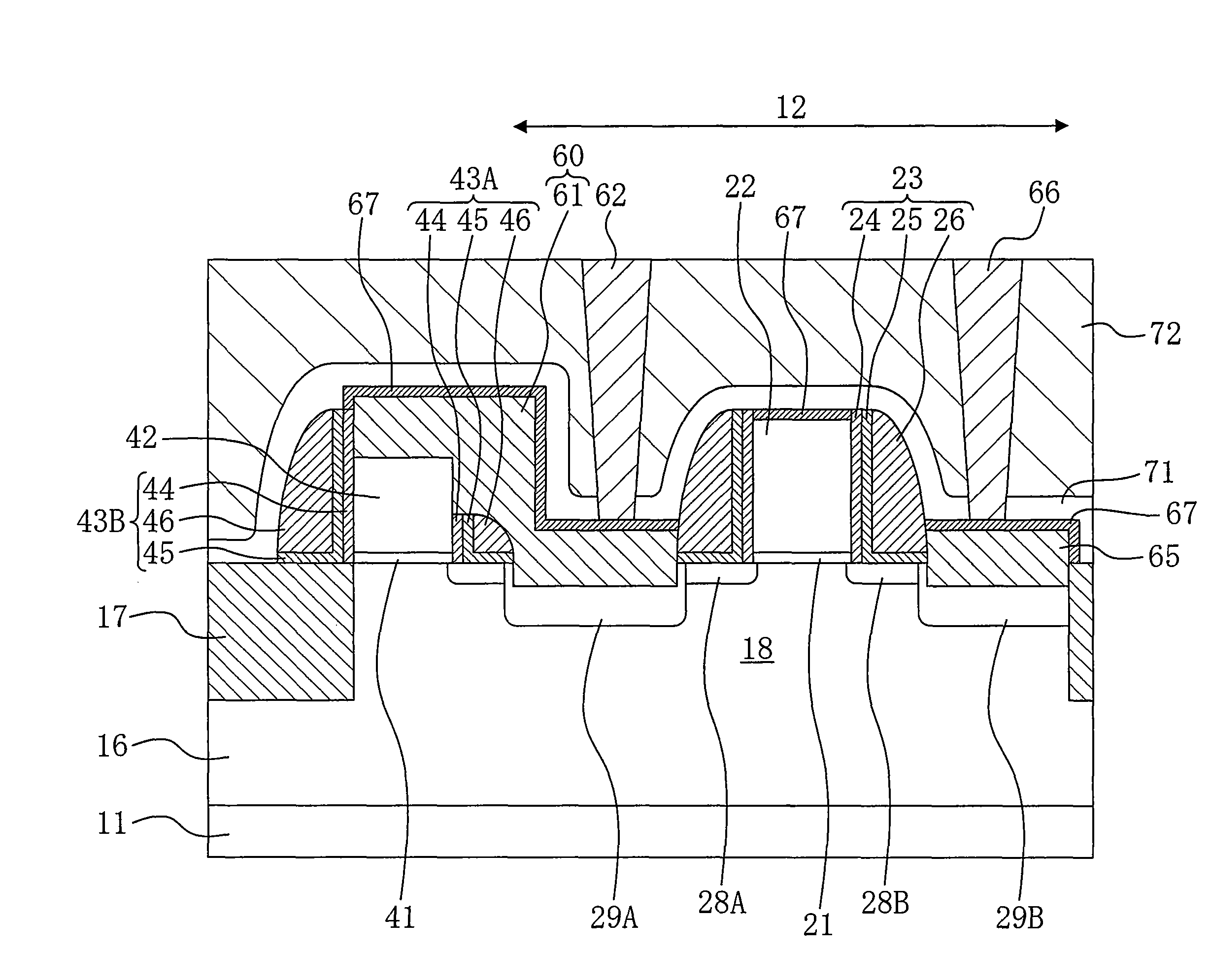
[0030]FIG. 1 shows a cross-sectional configuration of a semiconductor device of Embodiment 1 of the present invention. As shown in FIG. 1, the semiconductor device of this embodiment has a local interconnect structure 60 composed of a SiGe layer 61 formed to extend over the top surfaces of a first source / drain region 29A, a sidewall 43A and a gate interconnect 42.

[0031]As shown in FIG. 1, an n-type well 16 is formed in a semiconductor substrate 11 made of silicon (Si), and an active region 18 surrounded with an isolation region 17 is formed in the n-type well 16. A p-type MIS transistor 12 is formed in the active region 18.

[0032]The MIS transistor 12 includes a gate electrode 22 formed on the active region 18 with a gate insulating film 21 interposed therebetween and sidewalls 23 formed on both side faces of the gate electrode 22. Each of the sidewalls 23 has an offset sidewall 24 having a plate-shaped cross-section, an inner sidewall 25 having an L-shaped cross-section and an outer...

embodiment 2

Alteration to Embodiment 2

[0065]An alteration to Embodiment 2 of the present invention will be described with reference to the relevant drawings. FIG. 9 shows a cross-sectional configuration of a semiconductor device of an alteration to Embodiment 2 of the present invention. As shown in FIG. 9, the semiconductor device of this alteration has a local interconnect structure 60 composed of a first SiGe layer 61A formed on the first source / drain region 29A, a second SiGe layer 61B formed on the gate interconnect 42 and a shared contact plug 63 connected to part of the first SiGe layer 61A and part of the second SiGe layer 61B.

[0066]With the above configuration, the second SiGe layer 61B on the gate interconnect 42 extends toward the sidewall 43A, narrowing the space between the first and second SiGe layers 61A and 61B. Hence, the contact hole for the shared contact plug 63 can be made small compared with the configuration without the second SiGe layer 61B.

[0067]In this alteration, also,...


PUM


Abstract

The semiconductor device includes: a transistor having a gate electrode formed on a semiconductor substrate and first and second source / drain regions formed in portions of the semiconductor substrate on both sides of the gate electrode; a gate interconnect formed at a position opposite to the gate electrode with respect to the first source / drain region; and a first silicon-germanium layer formed on the first source / drain region to protrude above the top surface of the semiconductor substrate. The gate interconnect and the first source / drain region are connected via a local interconnect structure that includes the first silicon-germanium layer.

Description

CROSS-REFERENCE TO RELATED APPLICATIONS[0001]This application claims priority under 35 U.S.C. §119 on Patent Application No. 2007-282678 filed in Japan on Oct. 31, 2007, the entire contents of which are hereby incorporated by reference.BACKGROUND OF THE INVENTION[0002]1. Technical Field[0003]The present invention relates to a semiconductor device having a local interconnect structure and a fabrication method for the same.[0004]2. Background Art[0005]In recent years, with the trend toward finer semiconductor devices, gate electrodes tend to have larger contact resistance and wiring resistance. To address this problem, a local interconnect structure is used to connect a gate electrode with a source / drain region to thereby reduce wiring resistance (see Japanese Laid-Open Patent Publication No. 2007-150244, for example). The local interconnect structure as used herein refers to routing, including a shared contact plug, that connects an element and an interconnect mutually without use of...

Claims


Application Information

Patent Timeline
Patent Type & Authority Patents(United States)
IPC IPC(8): H01L21/8234
CPCH01L21/28525H01L21/76895H01L21/823425H01L21/823468H01L21/823475H01L27/11H01L29/78H01L2924/0002H10B10/00H01L2924/00H01L21/28518H01L23/535H01L29/161
Inventor OOSUKA, TSUTOMUOGAWA, HISASHISATO, YOSHIHIRO
Owner PANNOVA SEMIC
Why Eureka
Try Eureka