Semiconductor device and manufacturing method thereof

Inactive Publication Date: 2006-08-03
FUJITSU SEMICON LTD
View PDF5 Cites 180 Cited by
  • Summary
  • Abstract
  • Description
  • Claims
  • Application Information

AI Technical Summary

Benefits of technology

[0024] According to the present invention, before the amorphous semiconductor film is converted into the polycrystalline semiconductor film by irradiation of the energy beam, the shielding film which reflects or attenuates the energy beam is formed below the amorphous semiconductor film. Thus, an interlayer insulating film and wiring below the shielding film are not directly exposed to the energy beam. Accordingly, deterioration of these interlayer insulating film and wiring by heat of the energy beam is prevented.
[0025] Such an advantage is favorably obtained particularly when a laminated insulating film having a low dielectric constant insulating film with poor heat resistance is formed as the interlayer insulating film described above.
[0026] Moreover, when copper wiring is formed as the wiring, copper crystals hardly regrow into a needle shape by heat. Thus, it is possible to prevent short-circuit between upper and lower copper wirings due to the regrown coppe

Problems solved by technology

However, in reality, some points have been noted, which include that an ON-state current is not improved as expected and that heat generated by an increase in power consumption becomes a problem.
Accordingly, disadvantages have been newly caused by the miniaturization.
Furthermore, in the case where a low dielectric constant insulating film is used as an insulating film which covers the wirings, since the low dielectric constant ins

Method used


Image

  • Semiconductor device and manufacturing method thereof
  • Semiconductor device and manufacturing method thereof
  • Semiconductor device and manufacturing method thereof

Examples


first embodiment

(1) First Embodiment

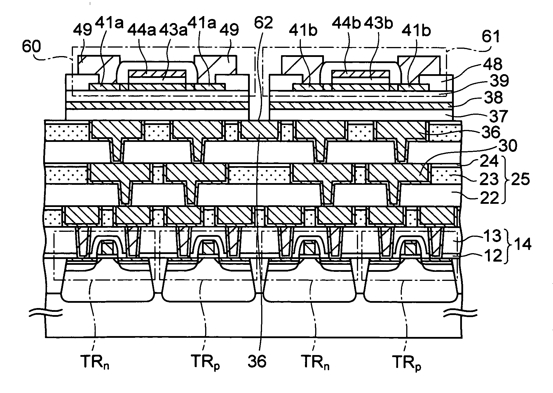
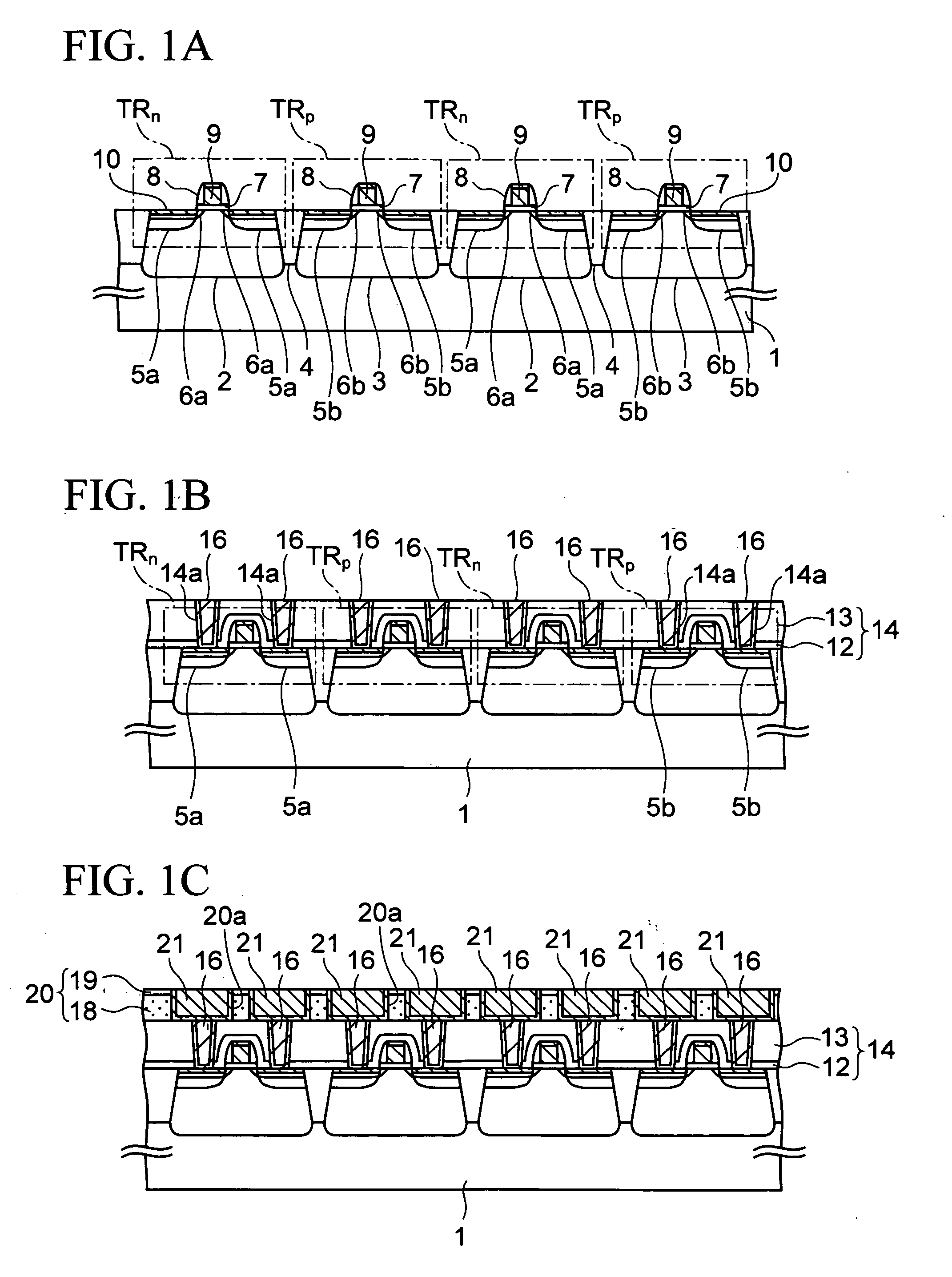
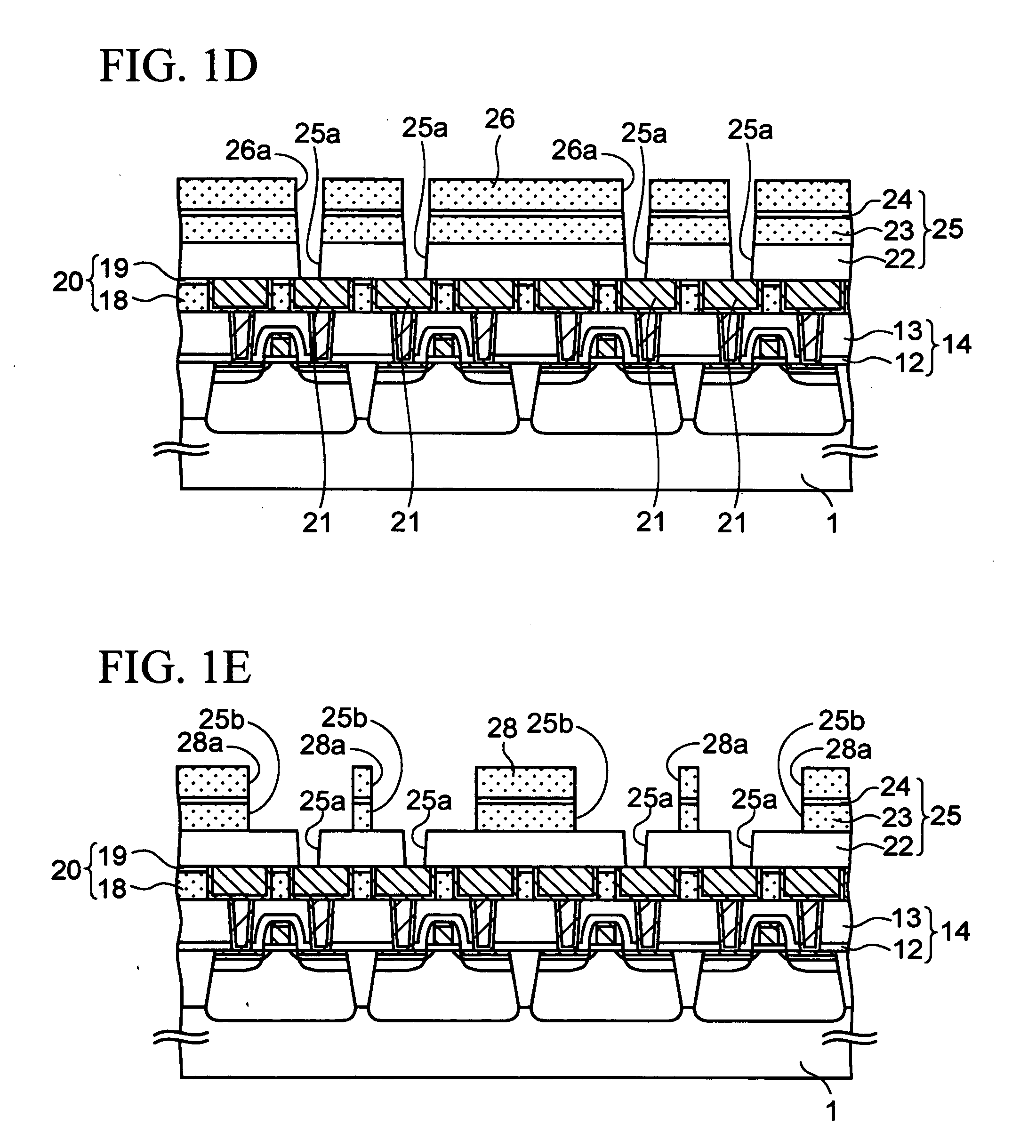
[0040]FIGS. 1A to 1S are cross-sectional views in the middle of manufacturing a semiconductor device according to a first embodiment of the present invention

[0041] First, description will be given of a step of obtaining a cross-sectional structure shown in FIG. 1A.

[0042] First, trenches for STI (shallow trench isolation) are formed in a silicon (semiconductor) substrate 1, and a silicon oxide film is buried in the trenches to obtain element isolation insulating films 4. Note that an element isolation structure is not limited to the STI but may be LOCOS (local oxidation of silicon). Thereafter, ion implantation of p-type impurities and n-type impurities is performed in transistor formation regions defined by the element isolation insulating films 4, thereby forming p wells 2 and n wells 3 in the silicon substrate 1.

[0043] Furthermore, after a silicon oxide film to be a gate insulating film 7 is formed by thermally oxidizing a surface of the silicon substrate 1,...

second embodiment

(2) Second Embodiment

[0125] In the first embodiment, the metal film such as the Al film is formed as a shielding film 38 in the step of FIG. 1H. On the contrary, in this embodiment, a reflecting film is formed as the shielding film 38 in the following manner.

[0126]FIGS. 6A and 6B are cross-sectional views in the middle of manufacturing a semiconductor device according to this embodiment. Note that, in FIGS. 6A and 6B, the components described in the first embodiment are denoted by the same reference numerals as those in the first embodiment, and description thereof will be omitted below.

[0127] First, description will be given of a step of obtaining a cross-sectional structure shown in FIG. 6A.

[0128] First, after the structure of FIG. 1G has been obtained according to the first embodiment, a reflecting film is formed to have a thickness of about 50 to 500 nm as shown in FIG. 6A, the reflecting film being obtained by sequentially laminating a nitride film (SiN film) and an oxide fi...

third embodiment

(3) Third Embodiment

[0136] In the first embodiment as already described, TFTs 60 and 61 having the LDD structure and the offset gate structure are fabricated. Meanwhile, in this embodiment, TFTs having a GOLD (gate overlap lightly doped drain) structure are fabricated.

[0137]FIGS. 8A to 8F are cross-sectional views in the middle of manufacturing a semiconductor device according to this embodiment. Note that, in FIGS. 8A to 8F, the components described in the first embodiment are denoted by the same reference numerals as those in the first embodiment, and description thereof will be omitted below.

[0138] First, description will be given-of a step of obtaining a cross-sectional structure shown in FIG. 8A.

[0139] First, after the steps of FIGS. 1A to 1M described in the first embodiment have been performed, a silicon oxide film is formed to have a thickness of about 30 nm on the entire surface by use of a plasma CVD method using vaporized TEOS as reactive gas. The silicon oxide film th...


PUM


Abstract

A method for manufacturing a semiconductor device, including the steps of: forming a shielding film 38 on a first insulating film 37; sequentially forming a second insulating film 39 and an amorphous semiconductor film 40 on the shielding film 38; melting the amorphous semiconductor film 40 at least in portions to be channels of thin-film transistors by irradiating an energy beam onto the amorphous semiconductor film 40, and converting the amorphous semiconductor film 40 into a polycrystalline semiconductor film 41; sequentially forming a gate insulating film 43a and a gate electrode 44a on the polycrystalline semiconductor film 41 on the channels; and forming source and drain regions 41a in the polycrystalline semiconductor film 41 on sides of the gate electrode 44a, and forming a TFT 60 by use of the source and drain regions 41a, the gate insulating film 43a, and the gate electrode 44a.

Description

CROSS-REFERENCE TO RELATED APPLICATIONS [0001] This application is based on and claims priority of Japanese Patent Application No. 2005-023968 filed on Jan. 31, 2005, the entire contents of which are incorporated herein by reference. BACKGROUND OF THE INVENTION [0002] 1. Field of the Invention [0003] The present invention relates to a semiconductor device and a manufacturing method thereof. [0004] 2. Description of the Related Art [0005] In recent years, semiconductor devices such as LSIs have been more and more miniaturized, and a gate length of a MOS transistor is becoming shorter than 90 nm. Along with such miniaturization, improvement in performance such as a shortened gate delay time is expected. However, in reality, some points have been noted, which include that an ON-state current is not improved as expected and that heat generated by an increase in power consumption becomes a problem. Accordingly, disadvantages have been newly caused by the miniaturization. [0006] Consequen...

Claims


Application Information

Patent Timeline
IPC IPC(8): H01L27/12
CPCH01L21/76807H01L21/84H01L23/53228H01L23/585H01L27/12H01L2924/0002H01L2924/00
Inventor HARA, AKITO
Owner FUJITSU SEMICON LTD
Why Eureka
Try Eureka