

Thin film forming apparatus cleaning method
a technology of thin film and cleaning method, which is applied in the direction of drying solid materials, drying, light and heating apparatus, etc., can solve the problems of negative influence on the global environment, and achieve the effect of suppressing the deterioration of the reaction vessel and the jig
- Summary
- Abstract
- Description
- Claims
- Application Information
AI Technical Summary
Benefits of technology
Problems solved by technology
Method used
Image

Examples
example 1
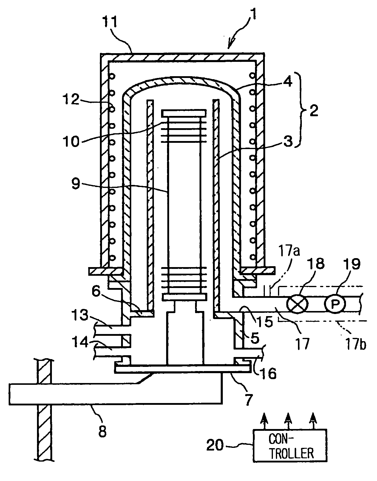
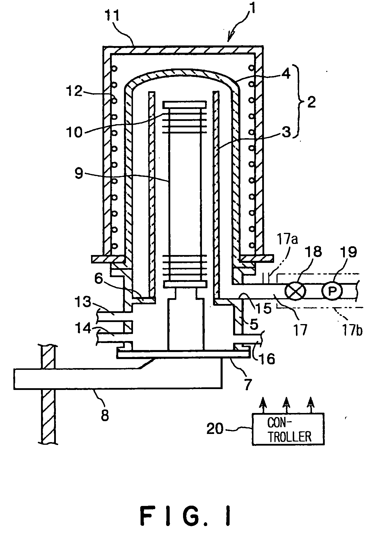
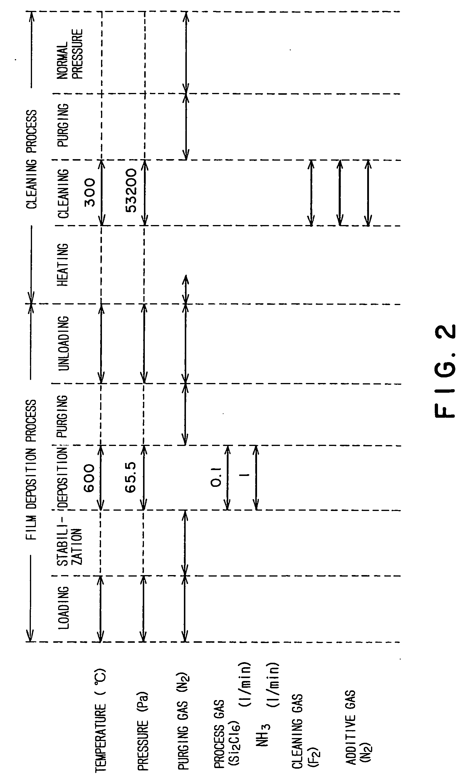
[0092] In a thin film deposition apparatus cleaning method in Example 1, fluorine gas, chlorine gas and nitrogen gas are supplied at 2 l / min, 0.35 l / min and 8 l / min, respectively, that is to say, a cleaning gas is supplied at 10.35 l / min through the cleaning gas supply pipe 14 into the reaction tube 2. FIGS. 3 to 5 show measured etch rates, and measured Si3N4 selectivities when the specimens were cleaned by the thin film deposition apparatus cleaning method in Example 1 using chlorine gas as an additive gas, together with those in a thin film deposition apparatus cleaning method in Comparative example 1 using a cleaning gas containing fluorine gas and nitrogen gas and not containing chlorine gas, and those in a thin film deposition apparatus cleaning method in Comparative example 2 using a cleaning gas containing fluorine gas and nitrogen gas and heating the interior of the reaction tube 2 at 400° C.
[0093] It is known from the comparative examination of data on the results of clean...
examples 2 to 5
[0100] In thin film deposition apparatus cleaning methods in Examples 2 to 5, cleaning gases containing HF gas are used as an additive gas. Etch rates and selectivities in Examples 2 to 5 were determined by a method similar to that of Example 1. In a thin film deposition apparatus cleaning method in Example 2, fluorine gas, hydrogen fluoride gas and nitrogen gas at 1.5 l / min, 0.5 l / min and 8 l / min were supplied respectively. That is to say a cleaning gas at 10 l / min in total into the inner tube 3 heated at 300° C. and maintained at a pressure of 53,200 Pa (400 torr). In the thin film deposition apparatus cleaning methods in Examples 3 to 5, cleaning gases having fluorine gas concentrations and hydrogen fluoride concentrations different from those of the cleaning gas used in Example 2 were used. In a thin film deposition apparatus cleaning method in Comparative example 3, a cleaning gas containing hydrogen fluoride gas and nitrogen gas was used and the reaction tube 2 was heated at 3...
examples 6 to 8
[0106] In thin film deposition apparatus cleaning methods in Examples 6 to 8, cleaning gases containing ammonia gas were used as an additive gas. Etch rates and selectivities in by Examples 6 to 8 were determined by a method similar to that in Example 1. In a thin film deposition apparatus cleaning method in Example 6, fluorine gas, ammonia gas and nitrogen gas at 1.78 l / min, 0.17 l / min and 8.05 l / min were supplied, respectively. That is to say, a cleaning gas was supplied in total at 10 l / min into the inner tube 3 heated at 300° C. and maintained at a pressure of 53,200 Pa (400 torr). In thin film deposition apparatus cleaning methods in Examples 7 and 8, cleaning gases having fluorine gas concentrations and ammonia gas concentrations different from those of the cleaning gas used in Example 6 were used. Measured data on the result of cleaning by Examples 6 to 8 is shown in FIGS. 9 to 11.
[0107] It is obviously known, from the comparative examination of data on the result of cleanin...
PUM
| Property | Measurement | Unit |
|---|---|---|
| flow rates | aaaaa | aaaaa |
| temperature | aaaaa | aaaaa |
| temperature | aaaaa | aaaaa |
Abstract
Description
Claims
Application Information