

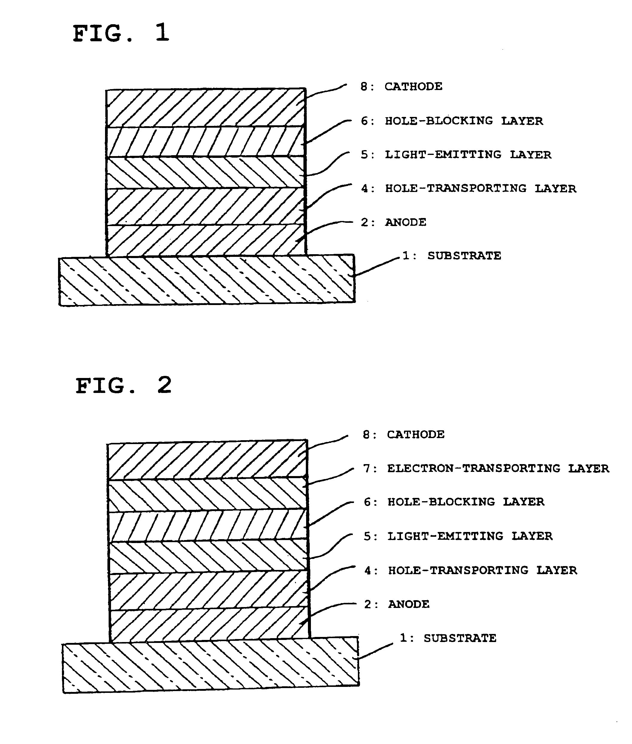
Organic electroluminescent device
a technology of electroluminescent devices and electroluminescent tubes, which is applied in the direction of discharge tube luminescnet screens, natural mineral layered products, etc., can solve the problems of difficult color emission, low luminance, and high cost of peripheral driving circuits, and achieve light emission efficiency, inhibit the deterioration of luminance, and high efficiency
- Summary
- Abstract
- Description
- Claims
- Application Information
AI Technical Summary
Benefits of technology
Problems solved by technology
Method used
Image

Examples
example 1
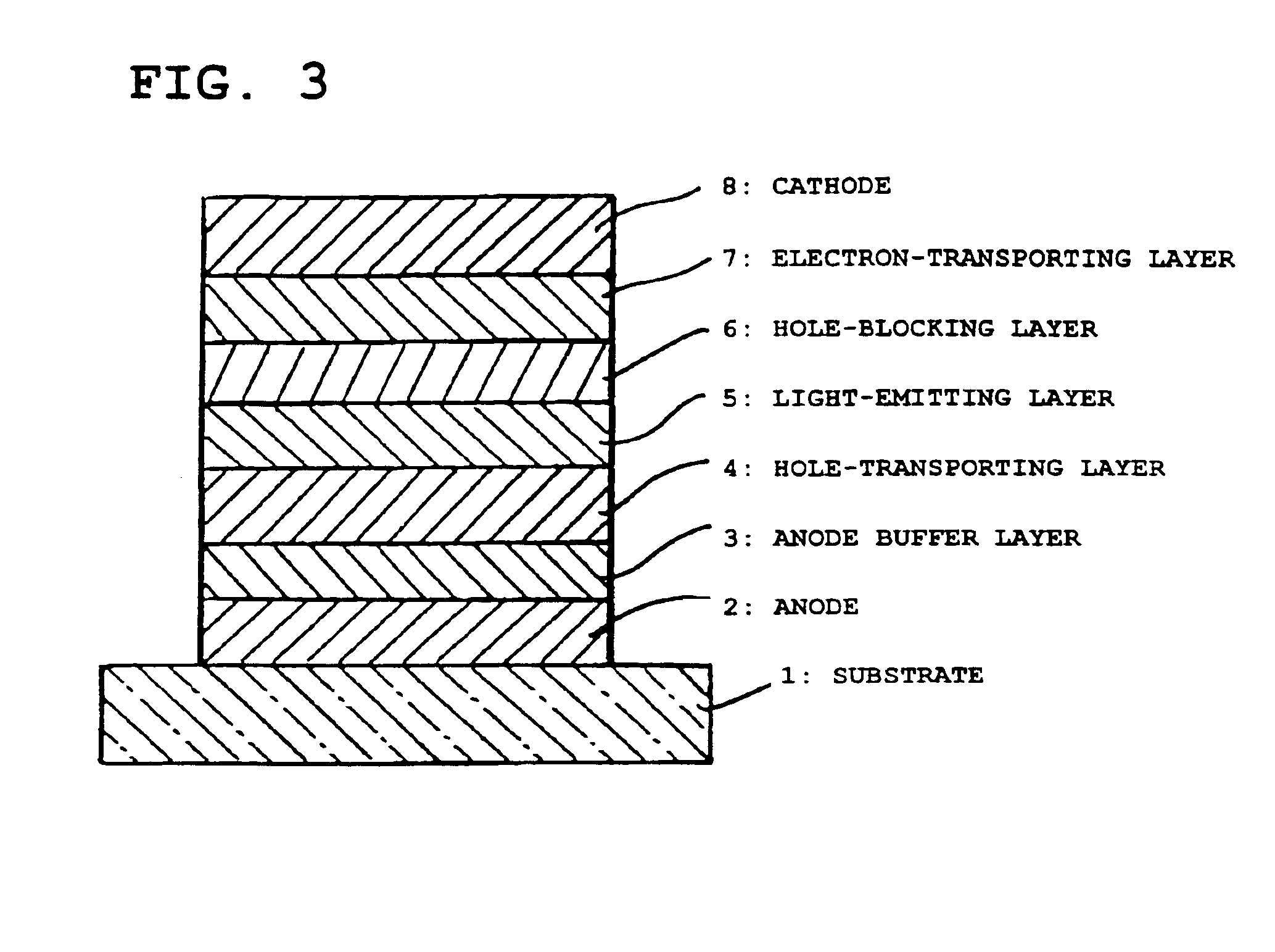
[0190]An organic electroluminescent device having a structure shown in FIG. 3 was fabricated by the following method.
[0191]A glass substrate 1 having deposited thereon an indium-tin oxide (ITO) transparent electrically conductive film to a thickness of 150 nm (an electron beam film formation product, produced by GEOMATIC; sheet resistance: 15 Ω) was patterned to have 2 mm-width stripes using normal photolithography technique and hydrochloric acid etching to form an anode 2. The ITO substrate after the pattern formation was washed in the order of ultrasonic washing with acetone, washing with pure water and ultrasonic washing with isopropyl alcohol, then dried by blowing nitrogen and finally washed with ultraviolet ozone. The thus-treated substrate was disposed within a vacuum vapor deposition apparatus and the apparatus was roughly evacuated by means of an oil-sealed rotary pump and then evacuated using an oil-diffusion pump equipped with a liquid nitrogen trap until the degree of va...
example 2
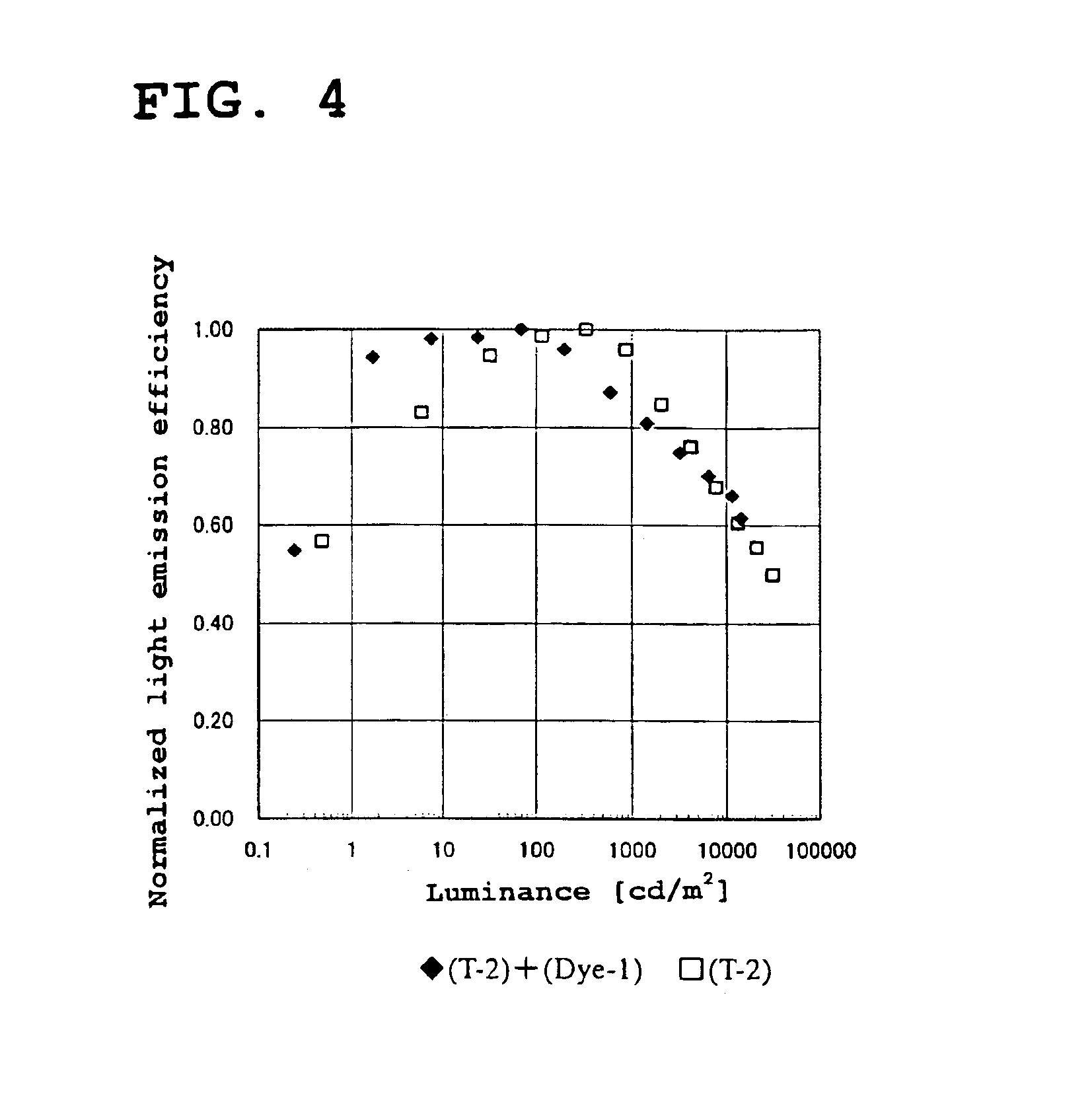
[0202]A device was fabricated in the same manner as in Example 1 except that Compound (H-34) was used as the main component of the light-emitting layer. The light emission characteristics of this device are shown in Table 3. The maximum wavelength of the light emission spectrum of this device was 585 nm similarly to Example 1 and identified as the wavelength attributable to Platinum Complex (T-8).
example 3
[0204]A device was fabricated in the same manner as in Example 1 except that Iridium Complex (T-17) was used in place of Platinum Complex (T-8) as one sub-component of the light-emitting layer. The light emission characteristics of this device are shown in Table 3. The maximum wavelength of the light emission spectrum of this device was 618 nm and identified as the wavelength attributable to Iridium Complex (T-17).
PUM
| Property | Measurement | Unit |
|---|---|---|
| thickness | aaaaa | aaaaa |
| thickness | aaaaa | aaaaa |
| transmittance | aaaaa | aaaaa |
Abstract
Description
Claims
Application Information