Light emitting apparatus and method for manufacturing the same

Inactive Publication Date: 2005-06-07
SEMICON ENERGY LAB CO LTD
View PDF42 Cites 135 Cited by
  • Summary
  • Abstract
  • Description
  • Claims
  • Application Information

AI Technical Summary

Benefits of technology

[0012]The purpose of the present invention is to solve the above problems in order to improve th

Problems solved by technology

A liquid crystal display apparatus is employed as an image displaying unit in various electronics, but suffers a problem that it has a narrow angled field of view.
However, it is difficult to form determined patterns on the organic electro-luminescence layer by photolithography technique as used in the semiconductor element manufacturing.
This prevents practical application of the light emitting apparatus comprising the light emitting elements.
When the organic compound has low melting point or glass transition temperature, the elect

Method used


Image

  • Light emitting apparatus and method for manufacturing the same
  • Light emitting apparatus and method for manufacturing the same
  • Light emitting apparatus and method for manufacturing the same

Examples


embodiment

Embodiment 1

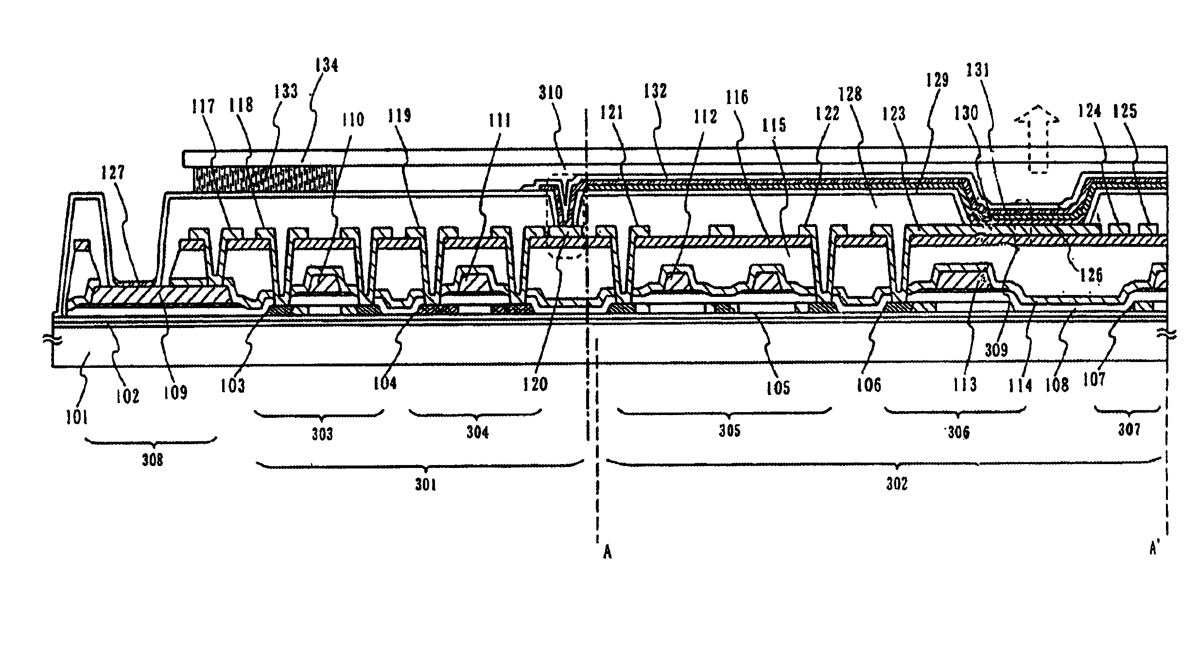
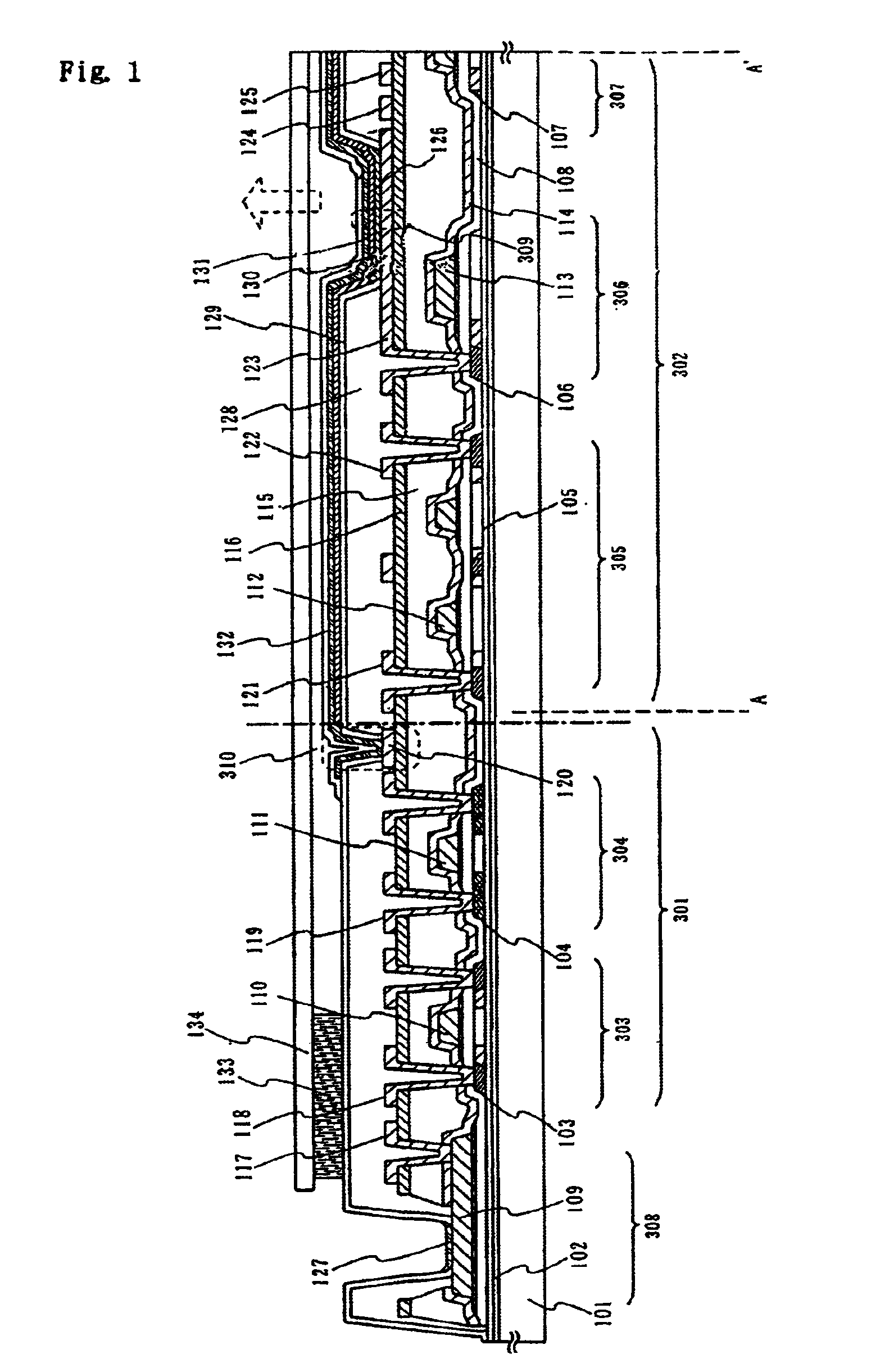
[0172]Next, the process of manufacturing the light emitting apparatus shown in FIG. 1 is described in detail with reference to the figures.

[0173]In FIG. 8A, the substrate 101 maybe one of a glass substrate, a quartz substrate or a ceramic substrate. The substrate 101 may comprise a silicon substrate, a metal substrate or a stainless substrate with an insulation film formed thereon. A plastic substrate having heat resistance bearable to the processing temperature of the embodiment may be used.

[0174]A first inorganic insulation layer 102 consisting of a insulation film such as a silicon oxide film, a silicon nitride film or a silicon oxynitride film (SiOxNy) is formed on the substrate 101. A typical example has two-layer construction, in which the first silicon oxynitride film of 50 nm thickness is formed using SiH4, NH3 and N2O as a reaction gas, and the second silicon oxynitride film of 100 nm thickness is formed on the first film, using SiH4 and N2O as a reaction gas.

[0...

embodiment 2

[0200]Next, a light emitting apparatus having different structure than that of the embodiment 1 will be described with reference to FIG. 14. The processes from the beginning to the formation of the third inorganic insulation layer 116 are same as those in the embodiment 1. Then, a contact hall and wirings 117 to 125 are formed.

[0201]Next, a third organic insulation layer 180 of about 1 μm thickness is formed of materials such as acrylic or polyimide. On this third organic insulation layer 180, a seventh inorganic insulation layer 181 is formed with silicon nitride for the same reason as the embodiment 1.

[0202]A contact hall connecting to the wiring 123 and a cathode layer 126 are formed. A fourth organic insulation layer 182 is formed at the end of the cathode layer 126 and the recess of the contact hall. The surface of the fourth organic insulation layer 182 is covered with an eighth inorganic insulation layer 183. After that, an organic compound layer 130 containing light emitting...

embodiment 3

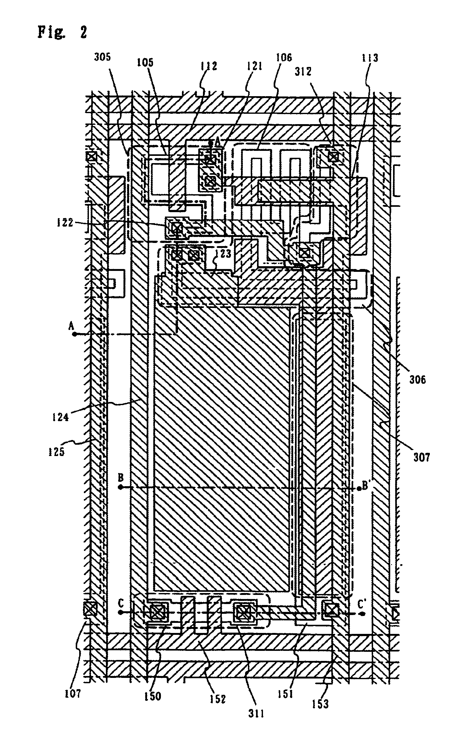
[0203]This embodiment has a different construction than that of the embodiment 1 for the pixel section, as illustrated in FIGS. 31 and 32. In this embodiment, the processes from the beginning to the formation of the third inorganic insulation layer 116 and wiring 123 on the third inorganic insulation layer 116 are same as FIG. 1.

[0204]As shown in FIG. 31A, a second organic insulation layer 180 covering the end of the wiring 123 is formed of a photosensitive, negative-type acrylic resin. Thus, the end where the second organic insulation layer 180 contacts with the wiring 123 has a inclined surface having a curvature as shown in the figure, the shape of which can be expressed by at least two curvatures R1 and R2. The center of the R1 is located above the wiring, while that of the R2 is located below the wiring. This shape may vary slightly depending on the exposure, but the thickness of the film is 1.5 μm and the value for R1 and R2 is 0.2 to 2 μm. The inclined surface has continuousl...


PUM


Abstract

The purpose of the invention is to improve reliability of a light emitting apparatus including a TFT and organic light emitting elements. The light emitting apparatus according to the invention having a thin film transistor and a light emitting element includes a first inorganic insulation layer on the lower surface of a semiconductor layer, a second inorganic insulation layer on the upper surface of a gate electrode, a first organic insulation layer on the second inorganic insulation layer, a third inorganic insulation layer on the first organic insulation layer, a wiring layer extending on the third inorganic insulation layer, a second organic insulation layer overlapped with the end of the wiring layer and having an inclination angle of 35 to 45 degrees, a fourth inorganic insulation layer formed on the upper surface and side surface of the second organic insulation layer and having an opening over the wiring layer, a cathode layer formed in contact with the wiring layer and having side end overlapped with the fourth inorganic insulation layer, and an organic compound layer formed in contact with the cathode layer and the fourth inorganic insulation layer and including light emitting material, and an anode layer formed in contact with the organic compound layer including the light emitting material, wherein the third inorganic insulation layer and the fourth inorganic insulation layer are formed with silicon nitride or aluminum nitride.

Description

BACKGROUND OF THE INVENTION[0001]1. Field of the Invention[0002]The present invention relates to a light emitting apparatus comprising a light emitting element which emit fluorescent light or phosphorescent light. In particular, the invention relates to a light emitting apparatus comprising an active element such as insulation gate type transistor or a thin film transistor, and a light emitting element coupled thereto.[0003]2. Description of the Related Art[0004]A typical display apparatus utilizing liquid crystal uses a back light or a front light for displaying images. A liquid crystal display apparatus is employed as an image displaying unit in various electronics, but suffers a problem that it has a narrow angled field of view. On the contrary, a display which uses light emitting elements providing electro-luminescence as a display unit has a wider-angled field of view as well as high level of visual recognition. These advantages make the electro-luminescent display prospective ...

Claims


Application Information

Patent Timeline
IPC IPC(8): H01L27/32H01L27/28H01L51/52H01L51/50
CPCH01L27/3244H01L27/3246H01L27/1248H01L27/124H01L51/5221H01L29/78621H01L29/78627H01L51/5253H01L2251/5315H01L2251/566H10K59/122H10K59/12H10K50/828H10K50/844H10K2102/3026H10K71/851
Inventor YAMAZAKI, SHUNPEIMURAKAMI, SATOSHISAKAKURA, MASAYUKITAKAYAMA, TORU
Owner SEMICON ENERGY LAB CO LTD
Why Eureka
Try Eureka